left is 1600 x 1131 pixels, perfectly legible.
A larger text could have allowed a 1000 wide pic to save size.
right is 2200 x 1555 pixels, a bit big, but legible.
You could crop all the unneeded surround/borders to save lots of pixels and with bigger text get down to that same 1000 wide.
But both can be seen with a little scrolling making them just acceptable.
Yes, better now. If you do have a way to crop, that's always helpful. So many CAD drawings have too much white space around them. Nice for a print, not needed for the web.better now?
You did well with the resize.

driver SPICE models
Mr. Zan, I'm playing with your suggestion of making TR=100n on AndyC & Dr.Dymond's models.
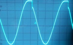
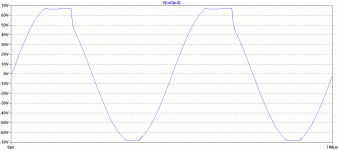
It would appear TR=400n matches Toni's results rather better. I enclose Toni's 'real life' pic of 20kHz overload and my sim with 2.285Vp input and TR=400n on 2sa1837/c4793_A.
TR=400n is roughly halfway between AndyC's 1.38u and your 100n
The 2.285Vp is unlikely to be what Toni used as his is a real amp with sagging PS rails. I give this number just for those who might want to replicate my sim.
May this bear with a small brain beg an explanation of TR in words of 1 syllable? 🙂 I take it changing TR has only small effect on other parameters.
____________________
Toni, would you say the 'real life' overload with 2sc5171/1930 is 'better' than 'real life' 2sa1837/c4793
Mr. Zan, I'm playing with your suggestion of making TR=100n on AndyC & Dr.Dymond's models.
It would appear TR=400n matches Toni's results rather better. I enclose Toni's 'real life' pic of 20kHz overload and my sim with 2.285Vp input and TR=400n on 2sa1837/c4793_A.
TR=400n is roughly halfway between AndyC's 1.38u and your 100n
The 2.285Vp is unlikely to be what Toni used as his is a real amp with sagging PS rails. I give this number just for those who might want to replicate my sim.
May this bear with a small brain beg an explanation of TR in words of 1 syllable? 🙂 I take it changing TR has only small effect on other parameters.
____________________
Toni, would you say the 'real life' overload with 2sc5171/1930 is 'better' than 'real life' 2sa1837/c4793
Attachments
Toni, would you say the 'real life' overload with 2sc5171/1930 is 'better' than 'real life' 2sa1837/c4793
First you are right - overload picture was taken from beginning overload - 2.3V peak may be correct. The power supply is a regulated one with overcurrent protection. I have taken the overload picture before the overcurrent protection has activated - so no sagging of PS rails has influenced the measurement.
The overload behaviour is optically nearly the same using 2SA1930 or 2SA1837 in VAS stage. Can't say which is the better one.
All I know is if we limit the maximum VAS current by increasing R22 up to 27R the overload betters significant - but also the THD is getting worse ...
@ astx
Hi, interesting that you use a trimmer in the LTP, as "some" have suggested not to !
How does affect THD etc ?
Hi, interesting that you use a trimmer in the LTP, as "some" have suggested not to !
How does affect THD etc ?
It would appear TR=400n matches Toni's results rather better. I enclose Toni's 'real life' pic of 20kHz overload and my sim with 2.285Vp input and TR=400n on 2sa1837/c4793_A.
TR=400n is roughly halfway between AndyC's 1.38u and your 100n
You have a pretty nice match. 100n was just a start value for the comparison with the real data from Toni.
May this bear with a small brain beg an explanation of TR in words of 1 syllable? 🙂 I take it changing TR has only small effect on other parameters.
It influences the total effective base to collector capacitance of a BJT, important mainly near saturation.
It controls the "extra" capacitance due to carrier sweep-out that adds to the depletion layer capacitance set by CJC.
Similar to the way the Ft of a transistor dominates the effective capacitance of the BE junction.
So, obviously important as the VAS clips but should have minimal impact on Andy's results to fit all the other parameters, if that is your concern?
Best wishes
David
@ astx
Hi, interesting that you use a trimmer in the LTP, as "some" have suggested not to !
How does affect THD etc ?
Not measured but maybe ignorable as only a very small part is controlled by trimmer. Needs investigation. Now due to better audio analyzer resolution it is possible for me to look at sub-ppm THD levels.
82R versus 580R bypass (330+ 1/2 of trimmers value).
Plan is to measure trimmer value after setup and replace by fixed resistors.
Astx,
you could unbalance the LTP emitter resistors and bring back the offset with trimming of R4 (the input Rin)
That way you could simulate for just the emitter resistor effect.
If the LTP trimmer needs an off centre adjustment, it is because the LTP is already out of balance. There are very many causes for this symptom and it would not seem reasonable to try to simulate for all the variations.
Astx,
you could unbalance the LTP emitter resistors and bring back the offset with trimming of R4 (the input Rin)
That way you could simulate for just the emitter resistor effect.
If the LTP trimmer needs an off centre adjustment, it is because the LTP is already out of balance. There are very many causes for this symptom and it would not seem reasonable to try to simulate for all the variations.
Even in simulation if we use exactly the same resistors and transistors (=best matched) there is a small imbalance/offset of about ~30mV (IMHO caused by base current of Q6 of about 6µA which leads to a small imbalance of CM).
We can tune this away by changing CM resistors or LTP resistors.
Attached simulations shows that tuning of Rin (R83 in sim/ R4 in schematic a few post ago) doesn't help us.
I know that there is minimum one well known person who demands to not use the LTP trimming and instead use a DC servo...
- Setting R14 and R52 to 70.00 we have about 34mV offset.
- Setting R14 to 70.41 and R52 to 70.00 we have tuned the offset nearly to zero.
BR, Toni
Attachments
I don't understand why that does not help.
If you have a completely balanced front end, then the output offset must be zero in the simulation because the simulator inserts identical resistors and identical transistors into the LTP.
If the LTP is not completely balanced, then it is likely one of the symptoms will be an output offset.
If you have that output offset, you can change the resistances on the +IN and -IN Pins to bring the offset to zero, or you can unbalance the emitter resistors to force the two transistor to compensate for the unbalance.
Neither method corrects the problem, the unbalance still exists. But you can make the symptom disappear.
So try again.
LTP trimming ...
Have temporarily removed LTP trimmer and set LTP degeneration resistors to 68R. (with trimmers LTP resistors are about 70R)
Distortion difference THD21k@200W@8R not really significant.
with trimmer:
0.00147 % bw 80kHz
0.00188 % no bw limit
without trimmer:
0.00143 % bw 80kHz
0.00184 % no bw limit
But note:
On the other hand: offset is due to good bjt matching and 1% resistor out of the box 6mV. Do we need any trimming here?
Have temporarily removed LTP trimmer and set LTP degeneration resistors to 68R. (with trimmers LTP resistors are about 70R)
Distortion difference THD21k@200W@8R not really significant.
with trimmer:
0.00147 % bw 80kHz
0.00188 % no bw limit
without trimmer:
0.00143 % bw 80kHz
0.00184 % no bw limit
But note:
- measurement digits are fluctuating +/- 0.2 ppm
- LTP resistors are about 1.5% lower as with trimmer
On the other hand: offset is due to good bjt matching and 1% resistor out of the box 6mV. Do we need any trimming here?
I don't understand why that does not help.
If you have a completely balanced front end, then the output offset must be zero in the simulation because the simulator inserts identical resistors and identical transistors into the LTP.
If the LTP is not completely balanced, then it is likely one of the symptoms will be an output offset.
If you have that output offset, you can change the resistances on the +IN and -IN Pins to bring the offset to zero, or you can unbalance the emitter resistors to force the two transistor to compensate for the unbalance.
Neither method corrects the problem, the unbalance still exists. But you can make the symptom disappear.
So try again.
you have forgotten the base current of Q6 of about 6µA which creates a small imbalance in the current mirror ...
I have not forgotten about base current.
A completely balanced LTP requires that the Vce is equal, that the Ie is equal, that the Ib is equal, and crucially that Tj is equal.
If you unbalance the LTP by injecting an extra current that is not matched by a current on the other leg then the symptom is likely to be output offset.
A completely balanced LTP requires that the Vce is equal, that the Ie is equal, that the Ib is equal, and crucially that Tj is equal.
If you unbalance the LTP by injecting an extra current that is not matched by a current on the other leg then the symptom is likely to be output offset.
Overload & TR
It makes the sim even closer to 'real life'. They were done with R22a+R22b=27R
What was R22 on the photographed amp?
Thanks for this Toni.First you are right - overload picture was taken from beginning overload - 2.3V peak may be correct. The power supply is a regulated one with overcurrent protection. I have taken the overload picture before the overcurrent protection has activated - so no sagging of PS rails has influenced the measurement.
The overload behaviour is optically nearly the same using 2SA1930 or 2SA1837 in VAS stage. Can't say which is the better one.
All I know is if we limit the maximum VAS current by increasing R22 up to 27R the overload betters significant - but also the THD is getting worse ...
It makes the sim even closer to 'real life'. They were done with R22a+R22b=27R
What was R22 on the photographed amp?
Toni's results with the 27 ohm VAS emitter resistor make perfect sense.
I used 11 ohms in my estimate so that may explain why it needed some adjustment.
This is where you say "Thanks Dave"😉
Best wishes
David
I used 11 ohms in my estimate so that may explain why it needed some adjustment.
...an explanation of TR in words of 1 syllable? 🙂
It influences the total effective base to collector capacitance of a BJT, important mainly near saturation...etc
This is where you say "Thanks Dave"😉
Best wishes
David
Last edited:
Have temporarily removed LTP trimmer and set LTP degeneration resistors to 68R. (with trimmers LTP resistors are about 70R)
Distortion difference THD21k@200W@8R not really significant.
with trimmer:
0.00147 % bw 80kHz
0.00188 % no bw limit
without trimmer:
0.00143 % bw 80kHz
0.00184 % no bw limit
But note:
We can't say removing the LTP trimmer betters THD by 0.2ppm ...
- measurement digits are fluctuating +/- 0.2 ppm
- LTP resistors are about 1.5% lower as with trimmer
On the other hand: offset is due to good bjt matching and 1% resistor out of the box 6mV. Do we need any trimming here?
im not sure this helps given how far advanced you are but jcx posted this on the Cordell book thread: http://users.ece.gatech.edu/~lanterma/sdiy/datasheets/transistors/AN-222.pdf
above Fig 6 it mention that the best way to null out initial offset in LTP is to trim the load resistors but not much details why. The referenced AN-3 may help explain but I cannot locate a copy. fwiw
I'll do better than that!This is where you say "Thanks Dave"😉
I grovel at your feet Oh Guru Zan 😱
Thanks for this Toni.
It makes the sim even closer to 'real life'. They were done with R22a+R22b=27R
What was R22 on the photographed amp?
12R.
im not sure this helps given how far advanced you are but jcx posted this on the Cordell book thread: http://users.ece.gatech.edu/~lanterma/sdiy/datasheets/transistors/AN-222.pdf
above Fig 6 it mention that the best way to null out initial offset in LTP is to trim the load resistors but not much details why. The referenced AN-3 may help explain but I cannot locate a copy. fwiw
Thanks kasey197.
Maybe it would be better to tune DC offset by balancing CM. Has to be verified.
Based on that, I've changed TR to 260n on AndyC's 2sa1837/c4793_A and also Harry Dymond's 2sc1930/5171_d models in my copy of Toni's mylibs.lib"What was R22 on the photographed amp?"
12R.
Toni, the 'pure Cherry' version NEEDS R22 at 27R but compensates with even lower THD than the TMC/TPC versions. I'll post some THD sims in a bit.
Thanks & grovel grovel to Guru Zan ... 😱
- Home
- Amplifiers
- Solid State
- 2stageEF high performance class AB power amp / 200W8R / 400W4R