I have seen many Mambers testing their amplifiers with 20kHz and higher squarewaves. Some even use 100kHz and 200kHz squarewaves.
The HF content of a squarewave heats up the esr of the Output Zobel.Yes, the operator !
Far be4 the cap heats up the resistors produce holy smoke ...😉
I've done extensible full power tests using 20k, 50k, 100k and even 200k square and sinus ... needed a lot of new zobel resistors but never a fresh capacitor ...
...
No,you sent me this MKP10 but this don't fit well🙂🙂🙂🙂...
Sorry - my fault. You can recycle the MKP10 for the zobel directly mounted at speaker terminals.
BR, Toni
Me too.Far be4 the cap heats up the resistors produce holy smoke ...😉
I've done extensible full power tests using 20k, 50k, 100k and even 200k square and sinus ... needed a lot of new zobel resistors but never a fresh capacitor ...
Always smoke the zobel resistors(testing conditions,only)!
Never a burned capasitor.

Sorry - my fault. You can recycle the MKP10 for the zobel directly mounted at speaker terminals.
It doesn't matter, i can solve this easy.🙂
Last edited:
Reverse R67, R71, R75 => the mosfet gate stopper resistors need to be soldered the other way round to keep the wire-inductivity to gate as short as possible. 😱
R66, R70, R74 orientation looks OK.
BR, Toni
Last edited:
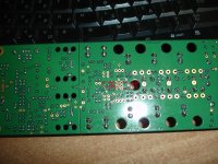
Exactly!like this?
R38 is a zero ohm resistor? If have soldered a piece of short circuit wire instead of R38 ...
Yes it is.Exactly!
R38 is a zero ohm resistor? If have soldered a piece of short circuit wire instead of R38 ...
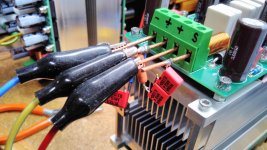
Nice scope friendly test socket at TP1 - where do you by this?This way?
BR, Toni
Some of them has been salvaged from an old pcb🙁Nice scope friendly test socket at TP1 - where do you by this?
BR, Toni
Thimios
Hi Toni,
I have some of these test points from Farnell, I believe. But, they are plentiful on Ebay. Here is an example. You can probably find more there.
50pcs Black Gold Tone Soldering PCB Board Breadboard Test Point Pin | eBay
Btw. I still haven't got around to start working on a fully balanced amplifier with N-channel outputs only. So if you find some of that spare time... 😛
Cheers,
Mogens
Toni my plan is to use one pair output transistor for first time
(soft) test.😉
Do you see any disadvantage in this practice?
(soft) test.😉
Do you see any disadvantage in this practice?
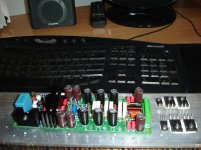
SA2015 first powering after assembling
Better to test fully assembled after double check all values. Diode orientations! Be carefully during MOSFET mounting! Use ESD equipment/procedures! Your MOSFETs triples are matched so don't mix them up.
Warning: due to a design error your PCB rev. 1.2 has no isolation from groundplane to mounting holes! Use isolation washers to avoid ground loops via heatsink!
Preparations be4 first power on:
Current should stay stable about 60mA per rail.
Both green leds should slightly glow.
Red bias led should glow.
Measured output offset should be about -17mV.
(Will settle later to near zero, if signal ground and power ground are connected to star ground in assembled amplifier)
Switch off immediately, if current limiter trips in! Scan for assembling errors.
Increase Voltage to +/- 20V. Resulting current consumption should be no more as about 80mA per rail.
Increase power supply current limit to 150mA
Increase Voltage to +/- 30V. Resulting current consumption should be no more as about 100mA per rail.
Increase power supply current limit to 600mA
Set bias with R41 clockwise until current consumption reaches about 450mA - 500mA. Check voltage between TP1 and TP3 - should be about 60mV (TP1 to TP2 about 30mV; TP2 to TP3 about 30mV)
If your amp is stable so far you can start your tests with dummy 8R load, sinus and square wave tests ...
Optimum bias is about 120 - 150mA per MOSFET pair so if you set total current consumption to about 450 - 500mA for your mean power supply voltage you are on the save side.
Use 2x30V AC toroids for your dc power supply. (~ +/- 41V DC)
Have fun,
Toni
Toni my plan is to use one pair output transistor for first time
(soft) test.😉
Do you see any disadvantage in this practice?
Better to test fully assembled after double check all values. Diode orientations! Be carefully during MOSFET mounting! Use ESD equipment/procedures! Your MOSFETs triples are matched so don't mix them up.
Warning: due to a design error your PCB rev. 1.2 has no isolation from groundplane to mounting holes! Use isolation washers to avoid ground loops via heatsink!
Preparations be4 first power on:
- wear safety glasses!
- set bias generator R41 trimmer to lowest bias (counter clockwise till end).
- no input connections / open inputs
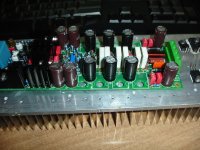
- add output zobel 4.7R + 47nF like attached picture. No load resistors attached!
- use laboratory power supply with voltage/current display and current limiting set to max. 80mA.
Current should stay stable about 60mA per rail.
Both green leds should slightly glow.
Red bias led should glow.
Measured output offset should be about -17mV.
(Will settle later to near zero, if signal ground and power ground are connected to star ground in assembled amplifier)
Switch off immediately, if current limiter trips in! Scan for assembling errors.
Increase Voltage to +/- 20V. Resulting current consumption should be no more as about 80mA per rail.
Increase power supply current limit to 150mA
Increase Voltage to +/- 30V. Resulting current consumption should be no more as about 100mA per rail.
Increase power supply current limit to 600mA
Set bias with R41 clockwise until current consumption reaches about 450mA - 500mA. Check voltage between TP1 and TP3 - should be about 60mV (TP1 to TP2 about 30mV; TP2 to TP3 about 30mV)
If your amp is stable so far you can start your tests with dummy 8R load, sinus and square wave tests ...
Optimum bias is about 120 - 150mA per MOSFET pair so if you set total current consumption to about 450 - 500mA for your mean power supply voltage you are on the save side.
Use 2x30V AC toroids for your dc power supply. (~ +/- 41V DC)
Have fun,
Toni
Attachments
Last edited:
I don't want to put on risk 6 matched trans.
I have two other pairs and i will try with these first.
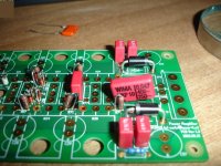
I'm confused a little in Vbe multiplier.
Is it this way as photo?
Should work stable even with a single pair OPS MOSFETs. Use the same startup procedure as described for 3 pairs except final max. bias current.
If you afterwards mount the matched 3 pairs don't forget to repeat the complete "first startup" procedure.
Bias generator parts mounting looks good so far compared to post #1408 and post #1422.
Mounting bias temp sensor parts is a bit tricky, but the pcb is held universal to allow different IPS and OPS variants.
BR, Toni
Thanks ,i see the post you mention but i can't see the link in jp4(between trans. and led) clear.Should work stable even with a single pair OPS MOSFETs. Use the same startup procedure as described for 3 pairs except final max. bias current.
If you afterwards mount the matched 3 pairs don't forget to repeat the complete "first startup" procedure.
Bias generator parts mounting looks good so far compared to post #1408 and post #1422.
Mounting bias temp sensor parts is a bit tricky, but the pcb is held universal to allow different IPS and OPS variants.
BR, Toni
BTW the multiplier emitter connected to led anode.
This way the Vbe trans. and led just touch the heatsink. Why do not use a BD139 screw firmly on the heatsink?
Last edited:
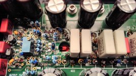
Ok,now is clearly visible.🙂Here a bias jumper J4 / led detail ...
Thanks.
Just now i found this.test points | Mouser Electronics, Inc.
Thx for link!
Hi Toni,
I have some of these test points from Farnell, I believe. But, they are plentiful on Ebay. Here is an example. You can probably find more there.
50pcs Black Gold Tone Soldering PCB Board Breadboard Test Point Pin | eBay
Btw. I still haven't got around to start working on a fully balanced amplifier with N-channel outputs only. So if you find some of that spare time... 😛
Cheers,
Mogens
Thx for link! Why using only N-Channel outputs? P-Channel vertical and lateral MOSFETs are still available.
If you want to go for only N-Channel MOSFETs maybe use a class D amplifier.
Hi Toni,
Well, actually only for the fun of it. The N-Channel and P-channel doesn't seem to be that complementary so I thought it could be fun trying to see what could be obtained by using N-Channel output stage only.
In reality, any of your designs are more than good enough. But, there is always a new mouse-trap 😀 We will see if and when I get this started.
Cheers,
Mogens
- Home
- Amplifiers
- Solid State
- 2stageEF high performance class AB power amp / 200W8R / 400W4R