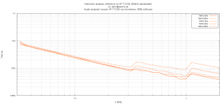
Distortion analysis for current improvements
2SC4793/2SA1837 are biased with R17=33R, C16=470nF
TMC compensation 68p/470p/1k
The first plot is the loop measurement of the analyzer itself for comparison.
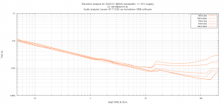
2SC4793/2SA1837 are biased with R17=33R, C16=470nF
TMC compensation 68p/470p/1k
The first plot is the loop measurement of the analyzer itself for comparison.
Attachments
Since the measured THD is significantly larger than the simulated THD (AFAIK), I think the layout needs to be improved, or higher quality resistors used. What resistors do you use for the feedback network and elsewhere in the signal path? You might take a laminated (with tape) piece of grounded foil and slide it between components at sensitive nodes to see if it affects THD. IE between the VAS and frontend, perhaps between the VAS and its buffer. Do you have a metal box you could sit on the frontend to see if magnetic shielding is helpful?
Since the measured THD is significantly larger than the simulated THD (AFAIK), I think the layout needs to be improved, or higher quality resistors used. What resistors do you use for the feedback network and elsewhere in the signal path? You might take a laminated (with tape) piece of grounded foil and slide it between components at sensitive nodes to see if it affects THD. IE between the VAS and frontend, perhaps between the VAS and its buffer. Do you have a metal box you could sit on the frontend to see if magnetic shielding is helpful?
Dear keantoken,
my THD analyzer is on it's own limits if you compare the two graphs. Also this analyzer is only able to measure THD+N.
E.g.: the oscillator of the VP-7723D produces at 0 dBV output level and 21 kHz a distorted sinus of 0.0020% THD+N (measured and verified with a HP8903B independently). If we send this distorted signal through the amplifier which produces 200W@8R with this input level we measure 0.0032% THD+N. As we can not do simple maths and say
0.0032 - 0.0020 = 0.0012
the only thing I can do now is to compare the db distance from fundamental to H2/H3 from input and output levels with my spectrum analyzer HP3585A (measurement range 100dB) and to see if there are more/new harmonics visible.
I think we can say that the distortion plot has to be interpreted as THD+N is minimum as good as seen on the plot or even better.
Can someone lend me an AP supa dupa analyzer? 😉
All used resistors are low inductive metal film 1%.
Power resistors are low inductive MPC74 type matched to 1-2%.
Input caps are of high quality MKP paralleled to reduce inductive component. Have you checked the PCB design from post #8 with gerber view program? Any recommendations?
BR, Toni
Cordell's distortion magnifier does the job.
It subtracts the distorted input signal from the amplified output signal to leave a clearer estimate of the residual.
It's in his book and in Jan's Linear publication.
It subtracts the distorted input signal from the amplified output signal to leave a clearer estimate of the residual.
It's in his book and in Jan's Linear publication.
Cordell's distortion magnifier does the job.
It subtracts the distorted input signal from the amplified output signal to leave a clearer estimate of the residual.
It's in his book and in Jan's Linear publication.
Dear Andrew,
thanks for information. I have the book and also Jan's Linear Audio Publications. It seems I have to build his DM. 😉
BR, Toni
nice idea to build discrete Darlingtons. To get them stable would be a challenge ...
Need to simulate this.
Thanks for the SPICE circuit. Probably a bit too late for you to adopt but it would fix the driver emitter resistor problem too!
Then you would not have to work out Keantoken's derivation of the values😉 There is an excellent step by step explanation of this in the Cordell book.
Best wishes
David
Thermal circuits can be modeled in SPICE, and it is likely just as helpful here as it is in actual electronics. Since thermal circuits are not very complex, at least for amplifiers, once one gains some understanding of thermal design, you can work it out without SPICE.
Thanks for this Toni. I enclose THD & 20k residual plots for this.from #274
2stageEF_class_AB_power_amplifier.asc
The attached LTSpice file includes all of our small changes.
This TMC is the best of the TPC/TMC versions. Still not as good as the Cherry version in #182 or your #274 converted to Cherry at 20kHz.
I'll write more about earthing later.
This will be HUGE! I'm very wary of anything that will charge up on overload and may be slow to discharge.keantoken said:C16 should be at least around 5 times the combined Cbe of the outputs. The time constant of C16 and R17 should be at least 5 times the max risetime expected.
In a commercial design, it is more important to guard against stupid or drunk users than to seek the last 1ppm THD or even pedantic theoretical justifications 😱 ... not that I'm accusing Kean of being a pedant 😀
Thermal circuits can be modeled in SPICE, and it is likely just as helpful here as it is in actual electronics. Since thermal circuits are not very complex, at least for amplifiers, once one gains some understanding of thermal design, you can work it out without SPICE.
Would be a nice theme for a new thread about thermal simulations ... 🙂
BR, Toni
This will be HUGE! I'm very wary of anything that will charge up on overload and may be slow to discharge.
In a commercial design, it is more important to guard against stupid or drunk users than to seek the last 1ppm THD or even pedantic theoretical justifications 😱 ... not that I'm accusing Kean of being a pedant 😀
No panik. 😎
After many stepped simulations I decided to use 470nF/33R. It's a good compromise.
Also my philosophy: I want to have the best THD figures but not the last ppm at the price of loosing stability and/or safety.
Some words to the removed bias cap C11 which I have now reintroduced: without a cap distortion rises measureable! Your introduced 1nF (C13) does not help enough to compensate this.
(bias cap C11 should be minimum 100nF to 1µF).
Waiting on your Cherry variant... 😉
BR, Toni
Forgot to tell you some about position of suckout cap on PCB.
In my first PCB design the suckout cap C16 was located at end of PCB paralleled with R17. The correct position for lowest THD is directly between upper and lower driver bjt's. The resistor R17 can remain far away at the other end of pcb and is working as "line" terminator. This bettered the square wave figure another time!
BR, Toni
Well, when I said that I was trying to make the point that the required capacitor will be huge but the driver bias can't possibly be adequate to discharge it quickly... Only I was being so subtle I didn't say that at all. 
I say a factor of 5 times because this is generally accepted as "swamped" for engineers. I found in practice I preferred a 1uF high quality cap for a double EF output stage with one pair of outputs. A much smaller cap would have been sufficient for the desired improvement in behavior, and less risky.
astx's 68R/470n driver bias has its Fc at 5KHz, right in the middle of audio. So, as long as the output stage is audible in some way, this cap must be important to the sound. Apparently I liked to move it down to 500Hz or so, which I think is the impedance dip of my speakers.
This is all to say that this cap isn't necessarily needed; its purpose is to allow the drivers to share the load during transients. If the drivers go into class AB however we get charge pumping and possible self-destruction.
I think a better way to tackle this problem is to ask, what is the problem we are solving with this cap? Why don't we just measure that problem and select the best value based on that?
Some have said that the cap was only necessary for the earlier amplifier designs because of the enormous Cbe and slowness of the transistors, and that the original designers would not have added this cap if they had had modern devices.
Because the audible effect of the cap seems to make it larger than it needs to be, I consider what its effects are at listening levels. In a common-emitter driver stage I designed, I found this cap was much more crucial for dynamic bias stability. This is not obvious in simulation unless you use dynamic signals, and I made my own sine-burst type signal to test dynamic bias stability in simulation.
The bias null point in a BJT output stage only works if it is maintained well. Dynamic excursions can easily upset the bias point without the need for thermals, and this effect can be instant without thermal delays - meaning a source of high-order distortion. The null point is specified as an optimal degeneration voltage across the emitter resistors, so this is what we should measure under dynamic conditions. This is much easier in simulation.
If you measure the voltage across the emitter resistors during a sine-burst at full power, and zoom in to the bottom peaks, you'll see that the actual bias point wanders with a dynamic signal. This is what our cap needs to help with.
So the question is, when we size this cap for best dynamic bias stability, does bias pumping occur with worst-case conditions?
Attached image shows dynamic bias upset with a 1KHz+1.1KHz sine input. This uses a 100n cap at max output into 6R. Based on the simulation, it looks like modern outputs are fast enough they don't need much of a cap here. Rather it seems that too LARGE a cap causes dynamic bias sag, for instance 1u or 10u. 100n appears to be the right value, but is only a slight improvement from no cap at all.
It seems to me now that the size of this cap depends not on the outputs, but the drivers. This is because the output bias is largely the result of how the drivers react to the loading of the outputs. The effect is largely frequency-dependent, but all my results show an optimal Fc of over 20KHz for R64 and C8. What this means is that any capacitance across R64 causes bias pumping period, and it should NOT be considered to be a way of decoupling bias, because it does the opposite. Audio bias decoupling should be done at a high-impedance point before the drivers because the driver emitters are a very nonlinear low impedance point where the loading of the cap is worse than its filtering effect. The exception is that it helps the drivers share the capacitive load of the output stage, and for this reason, it results in a slight improvement if the Fc is kept over 20KHz.
When designing an amp then, it is best then to set R64/C8 to an Fc of 20-50KHz, and work on the rest of the amplifier. So, forget about making the cap 5 times larger than Cbe - that's useless. The cap's useful effects are only in the ultrasonic and RF range, and if it's made too large, the effect on audio is to cause dynamic bias modulation - which if desired for sound quality should be the LAST thing you do after designing the amp sanely.
Attachments
Last edited:
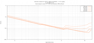
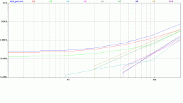
THD of Toni's #274 version
56.6Vp @ 8R
On 2EF274-20k.gif, I show 2 cycles of 20kHz at the equivalent level of 0.01% (blue) to give an idea of scale for the residual (red). Ignore the LF stuff.
Du.uuh!Thanks for this Toni. I enclose THD & 20k residual plots for this.
56.6Vp @ 8R
On 2EF274-20k.gif, I show 2 cycles of 20kHz at the equivalent level of 0.01% (blue) to give an idea of scale for the residual (red). Ignore the LF stuff.
Attachments

Last edited:
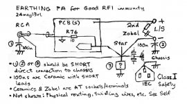
Earthing Power Amps for good RFI
All the amps I've designed & built use (3) ie Starpoint directly to Chassis. So I don't really know what to put in [?].
I'm now thinking its better to use (1) connect the input to Chassis as its easier and the 2 channels probably closer together too. Then the star point should probably have a 10R in [?]
I think the circuit should have ONE direct connection to Chassis. I don't like the idea of floating chassis like Cordell suggests.
For RF, EVERY lead that comes into the Chassis should be decoupled DIRECTLY WITH THE SHORTEST POSSIBLE LEADS to it.
I pontificate on this for a LN amplifier in the Yahoo MicBuilders Group as ricardo. You have to join.
I enclose how I think this should be done.Will RCA GND connect via zobel 0.1µF/10R directly to chassis. Or better to use only 0.1µF?
Speaker terminals: One 0.1µF/10R zobel directly between +/- terminals and one zobel from "-"terminal directly to chassis?
All the amps I've designed & built use (3) ie Starpoint directly to Chassis. So I don't really know what to put in [?].
I'm now thinking its better to use (1) connect the input to Chassis as its easier and the 2 channels probably closer together too. Then the star point should probably have a 10R in [?]
I think the circuit should have ONE direct connection to Chassis. I don't like the idea of floating chassis like Cordell suggests.
For RF, EVERY lead that comes into the Chassis should be decoupled DIRECTLY WITH THE SHORTEST POSSIBLE LEADS to it.
I pontificate on this for a LN amplifier in the Yahoo MicBuilders Group as ricardo. You have to join.
Hope that means you have two separate transformers too.Think of two complete monoblocks in one case.
see laterToday C17 will be desoldered!
I don't think so. But correct bandwidth limitation stops it from happening.Does the slew rate limit explain the constant frequency of the ringing? A small signal square wave has the same amount of steps inbetween 1µs window as a high level square wave (see pictures from post#252 ).
I don't know. This is new territory to me. At some point, you have to say, 'lets see what practical tests show'. I know 1R works cos you report this. In a while, if you have no problems with 0R47, we'll know if that's OK ... with matched hf + vbe of course 🙂do you think 0.47R driver emitter resistors are too low? Both drivers are matched to hfe + vbe.
Attachments
Last edited:
There is a ground loop between the RCA ground, PCB ground and chassis ground. R76 will prevent large currents from flowing through the PCB ground, but will convert these currents into voltage directly at the input. These currents will be induced by the trafo.
My question is, what are the specific RF problems that this method fixes?
My question is, what are the specific RF problems that this method fixes?
Only ONE of (1), (2) or (3) is connected directly to Chassis. Everything else is Starground. The pic doesn't show how you should twist transformer wires etc.There is a ground loop between the RCA ground, PCB ground and chassis ground. R76 will prevent large currents from flowing through the PCB ground, but will convert these currents into voltage directly at the input.
The pic sorta shows how Toni earths his present amp.
Are you recommending NO direct connection to Chassis? How would YOU earth his amp?
BTW, my scheme is fairly standard big Broadcast Mixing Desk practice, even if it's a simple unbalanced circuit.
ALL leads, including the screens on RCA cables, pick up RFI and conduct it directly inside the chassis. Even 1" of inside connection between the RCA GND and chassis is sufficient to give RFI in a sensitive circuit like a mike or phono preamp.My question is, what are the specific RF problems that this method fixes?
While a power amp is far less sensitive, you still see too many amps which click and pop .. or worse .. tell all & sundry that you have received a SMS on your phone. 😡
There's loadsa stuff in JAES jun95. Mostly with a professional balanced line level bias but lots that's applicable to a simple PA too.
If you mean magnetic induction, this generates an EMF, not a current. Here R76 takes up most of it so the voltage between 'clean' GND (RCA) and the star point is essentially '0'.These currents will be induced by the trafo.
Last edited:
Twisting trafo wires doesn't help much if the trafo itself radiates. Any loop of wire, especially a long one, becomes an antenna and will pick up this EMI and other RF signals.
The 10R resistor is there so that large currents would not flow from source ground to socket earth. Otherwise this connection can have very low resistance, and the large potential noise currents induce noise directly into the signal wire. A cable has plenty of mutual inductance. Shorting input ground to chassis ground circumvents this. At the same time it ensures a significant voltage cannot develop across the 10R resistor, as well as the possibility that noise from chassis ground will go into the input. In this case it may be better just to leave the 10R resistor out, as the damage is already done.
The 10R resistor is there so that large currents would not flow from source ground to socket earth. Otherwise this connection can have very low resistance, and the large potential noise currents induce noise directly into the signal wire. A cable has plenty of mutual inductance. Shorting input ground to chassis ground circumvents this. At the same time it ensures a significant voltage cannot develop across the 10R resistor, as well as the possibility that noise from chassis ground will go into the input. In this case it may be better just to leave the 10R resistor out, as the damage is already done.
- Home
- Amplifiers
- Solid State
- 2stageEF high performance class AB power amp / 200W8R / 400W4R