Hi Guys
Ranchu, if you look at Self's drawings both diode strings are in place. he went from a single diode to a pair in series to keep them from conducting in normal circumstances. As I've said, I've never had a situation arise that would have warranted them being there - just putthe positions on the board for anyone who wants them. Same with the cascodes et al.
Terry, if you remove the predriver then you remove all related components. Obviously this places a gap in the circuit, so two jumpers are fitted to get signal from the VAS to the drivers.
Similarly, if you remove the cascodes you remove all relatedcomponents (two Rs and a C) and then add two jumpers to get signal from the diff to the CM.
Power at higher or lower voltages is proportional by way of Ohm's law and the usual power equations.
Have fun
Kevin O'Connor
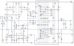
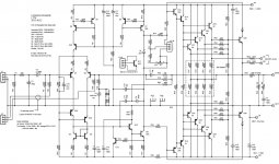
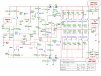
I am attaching a schematic showing the parts I removed and the jumpers. Can someone look at this and tell me what other, if any, parts need to be also removed?
I also added 2R2 SMD base stop resistors. I am just doing this on one of the three boards I have populated so I can test it.
Thanks, Terry
Attachments
Last edited:
Thanks Kevin, I'm pretty keen to get this working as an EF3, but if Terry has no preference then he would be well advised to take your advice and get it up and running as an EF2 with minimal board modifications.
Can you please tell me what software you used to lay out the Gerber files? I'm going to have a go at putting in some 1206 pads for base stoppers on the OP and drivers. While I'm at it I'll fix up the VBE tracks and add pads for C19. I want to retain the same board dimensions, standoff and OP locations so that I don't have to redrill my heatsink.
Can you please tell me what software you used to lay out the Gerber files? I'm going to have a go at putting in some 1206 pads for base stoppers on the OP and drivers. While I'm at it I'll fix up the VBE tracks and add pads for C19. I want to retain the same board dimensions, standoff and OP locations so that I don't have to redrill my heatsink.
I am attaching a schematic showing the parts I removed and the jumpers. Can someone look at this and tell me what other, if any, parts need to be also removed?
Thanks, Terry
Terry, if you remove the pre-drivers as indicated in your schematic, then you are running it as an EF2, and in that case you might get away without the base stoppers on the OP transistors. I would remove and jumper the pre-drivers first, test, and then install the base stoppers only if you still have stability problems.
EDIT: your IPS is not right. If you remove IP cascodes you also need to remove R52, R53 and C10. Do not replace with jumpers. You need to jumper the emitter-collector pads where Q28 and Q29 previously occupied, as you have correctly indicated on your schematic.
Last edited:
Too late, I already cut the traces and install the base stoppers. I am getting oscillation especially with a load attached. I only removed the items shown on the schematic. Basically what I listed above, D3, D4, Q28. Q29, Q13 & Q14. I didn't remove any resistors yet. Kevin said I should remove related parts but I don't know which ones are solely related to the transistors I removed.
Thanks, Terry
Thanks, Terry
That's okay... installing the base stoppers won't do any harm. Did you use 2.2 ohm as indicated on your schematic?
Is the DC offset under control now? Have you adjusted the trimpot to set ~29mV bias. Kevin has conveniently placed two pads (M1 and M2) that you can probe when setting bias.
The related parts are R52, R53 and C10. But please wait for a second opinion as I'm no expert.
Is the DC offset under control now? Have you adjusted the trimpot to set ~29mV bias. Kevin has conveniently placed two pads (M1 and M2) that you can probe when setting bias.
The related parts are R52, R53 and C10. But please wait for a second opinion as I'm no expert.
Last edited:
Yes, I used some 2R2 1/8W SMD resistors that I had in my parts drawers. Tiny little things. I just cut the traces right at the edge of the solder pads and exposed a little of the trace and then soldered in the SMDs. I think I may have a bad output transistor. They seem OK but as soon as I push the bias a little it will jump and I get an ugly looking sine wave on the scope, even with no input. Also, I can play a sine wave through it that is not bad looking but as soon as I add a load the bias rises quickly and the sine wave on the scope get badly misshapen. I replaced the drivers and no change so I fear one of the outputs has a problem.
I hadn't pulled R52, R53 and C10 because I wasn't sure if they somehow affected Q1 & Q4. I will wait for further instructions.
I'll probably stay with EF3 if we can make it work. I just thought I would try this.
Blessings, Terry
I hadn't pulled R52, R53 and C10 because I wasn't sure if they somehow affected Q1 & Q4. I will wait for further instructions.
I'll probably stay with EF3 if we can make it work. I just thought I would try this.
Blessings, Terry
I hadn't pulled R52, R53 and C10 because I wasn't sure if they somehow affected Q1 & Q4. I will wait for further instructions.
they are just loading the CCS and are better removed from the board...
for the cascode trannies, after pulling them out, jumpering the collector emitter of these trannies should work...
Hi Guys
R52,53 and C10 are related to the cascode - remove them and leave their spots open if you are taking out the cascode.
Your base-stops are okay; other links/cuts okay.
As others have said, EF2 is more stable than EF3, although I've had no need for base stops with either.
Have fun
Kevin O'Connor
R52,53 and C10 are related to the cascode - remove them and leave their spots open if you are taking out the cascode.
Your base-stops are okay; other links/cuts okay.
As others have said, EF2 is more stable than EF3, although I've had no need for base stops with either.
Have fun
Kevin O'Connor
Terry, I used 22R driver base stoppers on my DX MkIII (another EF2 design) and it worked well.
This was based on AndrewT's recommendation at the time, whose opinion I hold in high regard.
This was based on AndrewT's recommendation at the time, whose opinion I hold in high regard.
I must say this has been a bit of a let down. I have built four other blameless based amps and they all sound lovely. I really had high hopes for this one. It has been one road block after another. I feel really bad that I sold my excess boards to friends I've made here. Hopefully we find a working solution. this may be the last time I build a design in which the designer hasn't actually tried it himself. A big thanks to all of you who have stuck with this.
Blessings, Terry
Blessings, Terry
you are truly blessed Terry, you have the most to learn from all the hurdles you have encountered, just have the patience to see thru the circuit and understand what makes it tick...
Kevin needs to come up with circuit revisions in view of the experiences of the past day or two....
i am a fan of cascodes from my positive experiences with the Super Leach amps...
Kevin needs to come up with circuit revisions in view of the experiences of the past day or two....
i am a fan of cascodes from my positive experiences with the Super Leach amps...
Hi Anthony,
You are right of course. These struggles have caused me to begin to see how things work. I am getting much better at reading schematics and even built the spice model. Jason had to tweak it for me but still........🙂
I like the idea of cascodes too. The only reason I pulled them here was to try to see if that was causing the problems. It is easy enough the reinstall later. My spice model works. Still not sure why the real life model doesn't. The only change that has had a positive affect has been removing D4 and reducing C4. I have 220uf C4 now and it still takes 10 seconds or so for the offset to settle. With the big cap in there it would take over a minute.
BTW, I changed out C4 and removed the diodes on another board but have another issue there to look for because it won't bias. I'll look for that today.
Blessings, Terry
Hi Guys
Since the drivers and outputs all have pretty high beta, the driver base current is typically under a milliamp. Even if betas dropped this current would still be only in the milliamp range, so 100R drops 100mV or so at full load. Not an issue. Higher R here aids stability.
As I've said before, all of these circuits have been built by me and others, just not on this specific board. None of the practices are new or unconventional and I've never needed base-stops on outputs regardless of the output configuration. I left them off because I've never needed them but should have included them on this board since there were other things included as options already. besides which, even though the overall layout is fixed by the board, there can be many variations due to device selection and mounting by a variety of builders.
The bias reg is totally traditional, but I haven't used it since '92. I use CFP bias regs or direct-current-monitoring types, but more than 50% of comments I see in this forum disfavour CFP bias regs - so, this has the usual one.
If the DC offset takes so long to settle, changing C4 to a lower value is not the way to correct it. That will introduce low-F THD. The CCS for the input stage should allow the front-end to start-up at a low rail voltage and maintain a close-to-zero output while everything else gets up to speed. I've never had that problem with this topology or any other.
Have fun
Kevin O'Connor
Hi Kevin,
I can't speak for any of your old builds. I wish you had built this board because although you haven't had some of these issues before, they are present here. This amp starts up with a very high positive offset and them gradually reduces until it is negative offset. The bigger C4 is the longer it takes. I have built three of these boards so far and they all display the same thing. This is with the input shorted. Thank goodness someone noticed the diodes causing an imbalance in the front end. Too bad we didn't figure that out before I replaced all of the small transistors three times. Self has a 220uf cap there. Hopefully when we get these working you can redo the Gerbers so others will benefit.
Blessings, Terry
Terry, I have a 2.2mF fitted to C4 and it doesn't take long for the DC offset to settle at all, ever since I pulled the protection diodes around this cap. I would say it settles to 40mV within a second or so. So I suspect something else is going on.
You sound frustrated but when you get this up and running you will feel very satisfied. It's all a learning exercise - as you say it's not like you need another amp! 🙂
I am actually in the process of building an EF2 version of Kevin's design on a spare DX blame mkiii board I had lying around. Carlos' design doesn't have all the cascades but apart from that the two topologies are remarkably similar - the main difference being that Carlos has put his stamp on the Linn design by playing with the C and R values.
The mkiii boards are just a bit more spacious and easier to rework.
Hi Christian,
I had 4.7mF in the third board I built because I had one and Kevin had suggested in the notes to use the largest that would fit. I'm not going to do any more with this board until I see that you have a working board. I am frustrated. I carefully assembled the boards, fired them up with a light bulb and variac and had a huge offset. So then I spent hours measuring and notating everything on a schematic only to be told that there is nothing wrong with the layout or the circuit and I must have done something wrong, so I replaced all of the transistors, and got no change. Again I was told that I must have something wrong so one by one I replaced them again. Same result. It wasn't until you fired up your boards that someone realized that maybe I was right all along. I even built a third board so I could double check everything again. I don't know why yours settles quicker than mine. Mine starts off with a pretty large positive offset at initial energize and with the large cap in C4 it takes several seconds to wind down and ends up about -30mv. My single ended JLH doesn't take that long to settle. All three boards do the same. The difference is now with D4 removed they settle to a reasonable level.
I'm sitting here looking at Kevin's schematic and the MKIII and I don't see how you are going to build Kevin's design on that PCB. Carlos has 6 transistors in the front end and Kevin has 9. Carlos has 4 transistors in the VAS and Kevin has 6. The output section is fairly close except Carlos included base stoppers and Kevin has additional R38-45, Q25&26 and D7&8. Looks like the VBE is wired differently too. I don't know how closely you followed the last MKIII thread but we discovered that the lifted ground scheme is wrong on the board. You need to cut some traces and add a couple jumpers to fix it. I am learning, which is what I want to do. Maybe when and if you get yours working correctly you can post a schematic with some voltages and maybe some Vbe measurements. I don't really want to pull any more parts until I know I need to.
Blessings, Terry
Attachments
Hi Terry
I'm waiting on some more parts for my LTT4 board and it will be a week before they arrive, and then I'll be preoccupied with house renos and family stuff. So it will be a few weeks before I can report further. That's why I moved to the MkIII boards - because I can make progress with parts I have on hand.
The topologies are fundamentally the same. The extra small signal transistors you see in the LTT4 schematic are all cascodes.
- Status
- Not open for further replies.
- Home
- Amplifiers
- Solid State
- 250w 8ohm amplifier