Just sitting back and watching. I have built 3 board now in an effort to get one to run like the sim, without success. It is beyond my understanding so allow me to wait until you guys figure it out. I have a lot of parts invested at this point so I am still hopeful we can make this fly.
Blessings. Terry
Blessings. Terry
So I went and bought a small battery powered transistor radio and did some testing. I set the dial nearly to the end stop at the lower end of the frequency spectrum and was greeted with some lovely static as expected.
With the power on and the amp at idle I waved the antenna around the toroidal and the tone changed (kinda like a pipping sound).
I then positioned the antenna close to the output transistors and a couple inches from the +ve and -ve power lines. With the amp idling and the offset reading ~10mV there was nothing from the radio apart from the normal static.
After a bit of probing around with the meter, the tone changed and I could hear another type of static through the radio. Sure enough the DC offset at the speaker jumped to 0.4V+ and the outputs started heating up...
The tone was definitely different to the "normal" static and different to the static induced by the toroidal. I'm not sure whether this static is proof of oscillation, or simply that the radio is picking up the heavy current draw - as evidenced by the heating of the outputs.
There seems to be no reliable way to reproduce this suspected instability. Sometimes probing M1 & M2 will do it, other times it will manifest when I move the probe lead back to the speaker out lead.
Just sitting back and watching. I have built 3 board now in an effort to get one to run like the sim, without success. It is beyond my understanding so allow me to wait until you guys figure it out. I have a lot of parts invested at this point so I am still hopeful we can make this fly.
Blessings. Terry
Terry, I would hold off stuffing any more boards until we get to the bottom of this suspected instability. The DC offset issue I experienced (almost certainly part of your problem too) has been resolved by removing the zener protection diodes from around the NFB cap.
Now that I've removed the current limiting resistors from the fuse holders I'm experiencing what seems to be signs of instability in the OPS.
A couple of board modifications had to be made and one of the compensation caps slung underboard. So if it transpires that base stoppers are required for the output transistors (which I suspect will be the case) then I will probably respin the boards - with Kevin's blessing of course.
i think that you better put in the output base stoppers now....4.7 ohms at 1 watt is ok...
I should be able to get away with 1/2 W?
There is no room on the board for TH resistors. I can fit 1206 SMT but I only have 500mW in the following values:
3k3, 3k9, 4k75
The 3k3 500mW should be OK?
Emitter resistor
Another piece of info for the resident gurus (AJT and Jason) to consider:
I can't dial in any voltage drop across the emitter resistors and maintain quiescient conditions. I set the trimpot at 1k and then slowly advance it with the meter probes clipped to M1 and M2. The meter reads precisely 0.0mV right up until "all hell breaks loose" and the Vdrop jumps to > 100mV (and climbing) and the OPS is overheating.
is that a 10 turn trimpot?
does the collector emitter voltage of Q11 increase as you decrease the 1k ohm trimpot?
at what point is the increase abrupt?
does the collector emitter voltage of Q11 increase as you decrease the 1k ohm trimpot?
at what point is the increase abrupt?
Base stoppers fitted
OK so I got out the Dremel, cut the tracks and soldered base stoppers as close as possible to the OP pins...
Good news is that the outputs are ice cold even after probing around with the meter that would have surely sent them into thermal overdrive previously 😀
Feeling confident I set to work on the trimpot. I still get 0.0mV bias until about 3/4 of its range. When the trimpot is at 0R the bias is only 7mV and the pre-drivers are getting very warm indeed (Drivers and outputs are still cold to the touch.)
All my resistances around the VBE are per the schematic. I'm thinking about dropping R13 to 1k and increasing R35 to 1k also. 😕
Anyway this is good progress today. I think we can conclude that the base stoppers are an essential addition.
OK so I got out the Dremel, cut the tracks and soldered base stoppers as close as possible to the OP pins...
Good news is that the outputs are ice cold even after probing around with the meter that would have surely sent them into thermal overdrive previously 😀
Feeling confident I set to work on the trimpot. I still get 0.0mV bias until about 3/4 of its range. When the trimpot is at 0R the bias is only 7mV and the pre-drivers are getting very warm indeed
(Drivers and outputs are still cold to the touch.)All my resistances around the VBE are per the schematic. I'm thinking about dropping R13 to 1k and increasing R35 to 1k also. 😕
Anyway this is good progress today. I think we can conclude that the base stoppers are an essential addition.

Thanks AJT. Really appreciate your help 😀
I'm a little worried that these 1/2 W resistors won't stand up under heavy load. The problem is these 1206 packages are about the biggest that will sensibly fit.
The other thing I worry about is the lack of driver base stoppers. This is something I have seen in designs from OStripper and Bonsai. I believe Bonsai goes one step further and has a cap to shunt HF to ground. Is this something I should "add" this to the board to ensure that it is unconditionally stable under all normal loads?
Perhaps its time to respin the PCB?
I have recommended base stopper locations on all output devices and their drivers and pre-drivers (if fitted) to many Members who are designing PCBs. It's easy to short them out when testing proves that 0r0 is OK.
Just as I have suggested degeneration resistor locations for the front end transistors.
And multiple pin pitch for capacitors
And test point loops for "safer" measuring of operational PCBs.
And orienting all electrolytics in the same direction.
Don't worry about 500mW limit for base stoppers.
1r0 and 500mApk of base current is only 50% of the resistor rating.
What is happening to the Output Device if it draws 500mApk through the base?
I would not experiment as high as 4r7. Try 2r2 and lower.
Driver base stoppers are typically 10 to 50 times these values.
Last edited:
Hi Guys
The diodes around the feedback cap are just 1N914s or similar, not zeners. They just protect the cap if output offset goes to significant levels, as it might with a shorted output device. Self always has these in place. I've never added them in my bulds and have not had any issues.
Note also that as mentioned previously in this thread and in the PDF, the input stage cascode(s) can easily be dispensed with and are not an integral part of the design. I don't use cascodes. Just thought some builders might wish to use input devices with low Vce and might need cascoding - easily omitted if not needed since most modern BJTs used in big PAs have sufficient Vce for the rails used here.
If the output triple is problematic it is easy to go to an EF2 simply by leaving out the predrivers.
In normal operation, there would be about 1v4 across R36, suggesting about 14mA through the drivers. At 60V rails this is 8w4 per driver, so a bit toasty but that's why they are on a hefty heat sink. Increasing R36 from 100 to say 220 is a compromise in driver heat versus HF clearing of the output device base capacitance charge.
Similarly, R35 will have about 2v8 across it and therefore about 6mA through the predrivers and 360mW diss per BJT at 60V rails. Going to 1k cuts idle current and diss in half.
Increasing C19 to 33pF or even 47pF might help stabilise the EF3. You could also try lifting it.
I guess I lead a charmed life when it comes to building amps. I blew up my first amp in high school but never again. Everything works fine, sometimes requiring a small adjustment here or there but nothing like what Terry has experienced here. I'm sorry my luck has not transferred along through the design.
As stated earlier, this layout is one of many possible, so I will not be offended if anyone wants to lay it out differently. Personally, I would take out the cascodes and use an EF2. The OIC works well and the local filter caps should be maintained at the highest values practical.
Base stops for the output stage have to conduct a current equal to the load current divided by output beta (50-100) further divided by the number of outputs (4). At 250W into 8R, peak output current is about 8A, so base current for each output device is about 20-40mA. A 5R will drop 100-200mV and dissipate 2-8mW, so an 1/8W device is fine. It was not the intention to make this circuit "high gain" nor "high frequency extended".
Have fun
Kevin O'Connor
I have some questions. As most of you know I am trying to learn and have very limited electronic experience aside from what I have learned here by building amps and asking questions so please don't think I am trying to "teach" anything.
Hi Guys
The diodes around the feedback cap are just 1N914s or similar, not zeners. They just protect the cap if output offset goes to significant levels, as it might with a shorted output device. Self always has these in place. I've never added them in my bulds and have not had any issues.
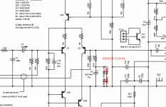
The diodes are not zeners but with them facing both directions don't they allow voltage to pass in both directions? NOTE: On one of my boards, with the diodes in place and a 4700uf cap in C4 the offset would start at +12vdc at initial turn on and gradually drop to -1.0vdc. I lifted on side of D4 and installed a 330uf 50V cap in C4. Now it starts at about +330mv at turn-on and settles quickly to -60mv.
Note also that as mentioned previously in this thread and in the PDF, the input stage cascode(s) can easily be dispensed with and are not an integral part of the design. I don't use cascodes. Just thought some builders might wish to use input devices with low Vce and might need cascoding - easily omitted if not needed since most modern BJTs used in big PAs have sufficient Vce for the rails used here.
To dispense with the cascodes I would pull Q28 & Q29 and short C-E on each?
If the output triple is problematic it is easy to go to an EF2 simply by leaving out the predrivers.
To do this, remove Q13 & Q14 and jump B-E on each? Any other changes? What about R35?
In normal operation, there would be about 1v4 across R36, suggesting about 14mA through the drivers. At 60V rails this is 8w4 per driver, so a bit toasty but that's why they are on a hefty heat sink. Increasing R36 from 100 to say 220 is a compromise in driver heat versus HF clearing of the output device base capacitance charge.
What about at 90V rails?
Similarly, R35 will have about 2v8 across it and therefore about 6mA through the predrivers and 360mW diss per BJT at 60V rails. Going to 1k cuts idle current and diss in half.
Increasing C19 to 33pF or even 47pF might help stabilise the EF3. You could also try lifting it.
C19 is not actually on the board, I had to add it.
I guess I lead a charmed life when it comes to building amps. I blew up my first amp in high school but never again. Everything works fine, sometimes requiring a small adjustment here or there but nothing like what Terry has experienced here. I'm sorry my luck has not transferred along through the design.
If I understand correctly, you never actually built this design. True?
As stated earlier, this layout is one of many possible, so I will not be offended if anyone wants to lay it out differently. Personally, I would take out the cascodes and use an EF2. The OIC works well and the local filter caps should be maintained at the highest values practical.
Base stops for the output stage have to conduct a current equal to the load current divided by output beta (50-100) further divided by the number of outputs (4). At 250W into 8R, peak output current is about 8A, so base current for each output device is about 20-40mA. A 5R will drop 100-200mV and dissipate 2-8mW, so an 1/8W device is fine. It was not the intention to make this circuit "high gain" nor "high frequency extended".
Have fun
Kevin O'Connor
well, we now know that those diodes were the cause of the output offset...
it is now confirmed that the amp did have some issues and is now debugged,
notably:
1. base stoppers for the output trannies are required
2. diodes across feedback cap is not really needed, there is enough
resistance in the circuit to protect the cap in case an output trannie fails...
i.e. the 47k ohm resistor plus the 1k in series limits the current to
less than 2mA to the cap in case of failure puts the rail at output node...
too small to cause significant damage...
my experience building amps.....
regarding output trannie failures, as you know semicon devices more
often than not fails as a short, and at times making the emitter resistors fail
as an open circuit....if the rail fuse did not blow soon enough....
Forward biased protection diodes
Terry, you need to remove D3 & D4. You can simply lift one of the legs or remove the diodes altogether for a more permanent fix.
The problem is that that these forward biased diodes steal current from the base of the LTP resulting in a large offset (~+3.4V in my case) at the speaker terminal.
You can leave D1 & D2 in place if you wish - they won't do any harm - and in fact Self has a reversed biased protection diode in his reference design.
Credit goes to AJT for reporting this problem many pages ago in this same thread.
I mistakenly referred to these diodes as "zener" diodes when they are most certainly not. I had a lot of my mind yesterday. Rest assured I've been testing with standard 1n4148 switching diodes at all times.
Attachments
Input stage cascodes
Terry, there is no problem leaving these transistors (Q28 & Q29) in the boards if you wish. Make sure you use PNP transistors (2n5401 or similar) and observe proper orientation as indicated on the silkscreen.
Terry, there is no problem leaving these transistors (Q28 & Q29) in the boards if you wish. Make sure you use PNP transistors (2n5401 or similar) and observe proper orientation as indicated on the silkscreen.
Hi Guys
Ranchu, if you look at Self's drawings both diode strings are in place. he went from a single diode to a pair in series to keep them from conducting in normal circumstances. As I've said, I've never had a situation arise that would have warranted them being there - just putthe positions on the board for anyone who wants them. Same with the cascodes et al.
Terry, if you remove the predriver then you remove all related components. Obviously this places a gap in the circuit, so two jumpers are fitted to get signal from the VAS to the drivers.
Similarly, if you remove the cascodes you remove all relatedcomponents (two Rs and a C) and then add two jumpers to get signal from the diff to the CM.
Power at higher or lower voltages is proportional by way of Ohm's law and the usual power equations.
Have fun
Kevin O'Connor
- Status
- Not open for further replies.
- Home
- Amplifiers
- Solid State
- 250w 8ohm amplifier