Agreed. But the output impedance and line rejection is much better in the case with the 1Meg resistor, because it employs no positive feedback to the SET pin. Simulations will bear this out.
I'm not seeing any issues with the LT3080 in the 21st Century Maida Regulator.I'm planning to use the LT3081 myself as it has very slightly better noise specs, bigger SOA, and a 50uA set current which should decrease problems associated with leakage.
Mouser now has LT/ADI components as well. You can buy them directly from ADI as well.Negative is that it doesn't come in the same package format, so I'll see what performance I can get using a TO-220 (LCSC.com has them for cheap in quantity).
Tom
Agreed. But the output impedance and line rejection is much better in the case with the 1Meg resistor, because it employs no positive feedback to the SET pin. Simulations will bear this out.
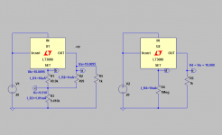
Yes.. le voila:
Attachments
Thanks for the simulations, jackinnj.
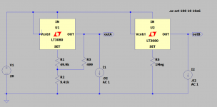
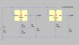
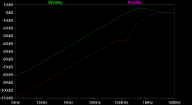
Consider any three-terminal regulator that employs an R3 : R2 feedback network such as one of the cases jackinnj shows above. Let's approximate the very high impedance of the SET pin (or ADJ pin in the case of an LM317) as infinite. We can define a feedback factor F equal to the voltage divider transfer function R2 / (R2 + R3).
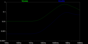
In the audio frequency range, the AC output voltage is almost equal to that at the SET/ADJ pin due to the internal loop gain of the regulator IC. In this range, output impedance and line rejection are degraded by a factor D = 1 / (1 - F) = 1 + R2/R3. The advantage is clear in the case where R3 is infinite and there is no feedback from regulator output to input. This is the best the regulator is capable of. If R3 must be used, it is best to keep R2/R3 as small as possible. If the feedback network contains capacitors, D will be the smallest if all component impedances in the Output to SET/ADJ path are kept as large as possible with respect to those in the ground to SET/ADJ path.
Starting somewhere above audio frequencies, the IC's internal loop gain falls enough that its AC output voltage is noticeably less than its input's. Here the degradation D is reduced by a small amount, but the advantage of zero or small amounts of feedback is still clear.
Consider any three-terminal regulator that employs an R3 : R2 feedback network such as one of the cases jackinnj shows above. Let's approximate the very high impedance of the SET pin (or ADJ pin in the case of an LM317) as infinite. We can define a feedback factor F equal to the voltage divider transfer function R2 / (R2 + R3).
In the audio frequency range, the AC output voltage is almost equal to that at the SET/ADJ pin due to the internal loop gain of the regulator IC. In this range, output impedance and line rejection are degraded by a factor D = 1 / (1 - F) = 1 + R2/R3. The advantage is clear in the case where R3 is infinite and there is no feedback from regulator output to input. This is the best the regulator is capable of. If R3 must be used, it is best to keep R2/R3 as small as possible. If the feedback network contains capacitors, D will be the smallest if all component impedances in the Output to SET/ADJ path are kept as large as possible with respect to those in the ground to SET/ADJ path.
Starting somewhere above audio frequencies, the IC's internal loop gain falls enough that its AC output voltage is noticeably less than its input's. Here the degradation D is reduced by a small amount, but the advantage of zero or small amounts of feedback is still clear.
Going back to post 150 -- too bad the On-Semi (Fairchild) H11FM can only be used to 30V -- can go to 300M Ohms -- for R7
I can't find a link to the H11FM - can you provide one?
In post 150, R7 = 10M ohms (not 300) gets you 300V.
I believe the successful use of such high resistances requires starting with a clean PCB (depending on the manufacturing process, the board may need to be cleaned post-soldering) and following up with an application of conformal coating to protect against humidity and contaminants.
I can't find a link to the H11FM - can you provide one?
In post 150, R7 = 10M ohms (not 300) gets you 300V.
I believe the successful use of such high resistances requires starting with a clean PCB (depending on the manufacturing process, the board may need to be cleaned post-soldering) and following up with an application of conformal coating to protect against humidity and contaminants.
Missed a digit, sorry. H11F1M, H11F2M, H11F3M -- take a peek at the Mouser site and select OnSemi photo-fet optocouplers https://www.mouser.com/datasheet/2/308/H11F3M-1306481.pdf
I assume you're looking to make an adjustable output voltage regulator. The LND150 (see attached) will give you the high voltage compliance you need. If you need more than 500V, The IXYS IXT? 01N100D ( ? = P, U or Y and selects package type) will extend things to 1000V. No guarantees as to the ease of setting the desired output by applying a given LED current, or the stability of the setting with temperature (although there should be negligible self-heating.) If you don't need an isolated driver, replace the MOSFET in the opto with a trimmer resistor.
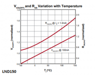
But even without self-heating, the problems with these solutions are the large temperature coefficients. Refer to the other LD150 attachment. The opto datasheet doesn't seem to have the requisite tempco data, but I expect it'll have the same problem.
Digikey has a 10M 19USD rotary potentiometer with a 19 week delivery time, and a 0.64USD 5Mohm trimmer in stock. You could cascade either of these with switched, fixed resistors.
Or you could just use the post 513 design with my Denali Voltage Reference, which is pretty darn stable with temperature. The Denali can be used with either the LT3080 or an LM317-based regulator. But I can conceive of a simplified version of the Denali which takes advantage of the LT3080 SET current feature.
Attachments
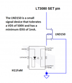
No guarantees as to the ease of setting the desired output by applying a given LED current, or the stability of the setting with temperature (although there should be negligible self-heating.)
You use two of the FET - couplers. I have done something similar with the Avago (was Hewlett Packard) HCNR-200. You can achieve excellent linearity.
https://www.edn.com/use-a-photoelec...as-a-linear-voltage-controlled-potentiometer/
I have tubes of DN2540 and scores of LND150 -- The BSP135 is a bit beefier, although only SMT.
Last edited:
Thanks for your mention of other small signal high voltage depletion MOSFETs.
Yes, I'm familiar with the technique that you referred to in the EDN article. I didn't think you wanted to go that far, as it requires an additional power supply for the op amp.
Also, what is needed here is not a variable current, but a variable resistance to work with the fixed LM3080 SET current. Even if you can cause the two opto MOSFETs to track characteristics, the impedance looking in the LND150 drains is dependent on them, the LND150 transconductances, and the LND150 drain-source resistances. Now you have to match LND150's.
You could use BJTs like the 400V Zetex ZTX458's to take advantage of the more repeatable BJT transconductances. If needed, the 400V limitation could be extended with series resistors or zeners or cascoded BJT's, the "top" BJTs' bases being fed from a voltage divider driven by the regulator output. But you'd still have to match the resistances between the collectors and the emitters.
I don't see how to get the tracking idea to work here because of the need to introduce high voltage matched transistors, but I could be missing something.
Maybe a variable resistor in the Gate-Source path of an LND150 would provide a simple acceptable solution.
Thoughts?
Thank you guys it's very interesting to read. I think I will buy the pcb to test.
I have a question: if you have the space for a choke, would you use a maida style reg over a clc filter stage ? If not, why ?
Thank you.
I have a question: if you have the space for a choke, would you use a maida style reg over a clc filter stage ? If not, why ?
Thank you.
Unlike a CLC, the Maida-style regulator establishes a very stable DC output voltage. This is to be desired unless the combination of high load current and low line voltage causes the rectified, filtered and unregulated input to the Maida to dip low enough to drive the regulator out of regulation. However, you should be able to design to prevent this. This is never a concern with a CLC alone.
You would need a complex, multistage CLC to approach the line noise rejection from DC through audio frequencies that the Maida-style regulator affords.
You would need a complex, multistage CLC to approach the line noise rejection from DC through audio frequencies that the Maida-style regulator affords.
Thank you guys it's very interesting to read. I think I will buy the pcb to test.
Sounds great. I have plenty in stock.
I have a question: if you have the space for a choke, would you use a maida style reg over a clc filter stage ? If not, why ?
Nah... Just let the regulator do its job.
Tom
Can lt3088 be used instead lt3080?
Different package, different I-Set
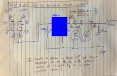
I have CLC PS in a low wattage 807 SE mono amp. I would like to "insert" a Maida requlator at location A.
Downstream of location A, and in parallel, are the OPT and a pair of OD3 gas tubes to feed front end tubes. Please take a look at the schematic, if you would.
Are there be any potential problems due to the downstream filter?

Downstream of location A, and in parallel, are the OPT and a pair of OD3 gas tubes to feed front end tubes. Please take a look at the schematic, if you would.
Are there be any potential problems due to the downstream filter?
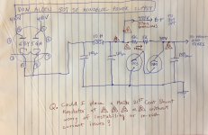
I would place the Maida Reg at point A in your schematic. You could even get rid of the 10H and second 100uF and just place the Maida Reg at the first 100 uF cap as I've shown in attached schematic.
I would design the Maida for 100 mA peak and 60 mA average (per channel) using the Excel sheet I provide with the board.
Tom
I would design the Maida for 100 mA peak and 60 mA average (per channel) using the Excel sheet I provide with the board.
Tom
Attachments
- Home
- Vendor's Bazaar
- 21st Century Maida Regulator