Why not use the I/V conversion method recommended by the official data sheet?
I think the resistors built into the AD1862 will be better.
Many of us have preferred resistor types that are a good fit for the desired sonic flavour. No idea how good the internal resistor is but somehow not holding my breath.
Yes, I used the I/V scheme shown on the datasheet.@CNOracle , do your board use the I/V design on the datasheet?
It works great.

Yes! This is probably the main factor.Not flexible. External resistor value can set the output voltage level from DAC 🙂
But the output level value of the internal resistor is suitable for most applications
Please forgive my not absorbing this threads nearly 600 pages. I am trying to mate the Miro 1.3 version of the board with JLSounds board, which is a newer galvanized isolated unit. The .pdf on their site and lack of DAC jargon has left me with a number of questions. It looks like the ideal board is the one with adapter and Opamps outputs, but I cannot find the gerbers for one that I have seen be created here recently. In any case, I could use a little help assuming I CAN hook up these two boards.
I am not sure what pins go where for Miro's 4,2...
Does the 11->4, and 15-2?
I wish to just do thse two things, and assume that jumpering the JLSounds board per screenshot will work H1.1->H3.17, H1.2->H3.19.
If someone can tell me if this setup will work good, and if so, if any errors (assumed) in my analysis.
You should try the 2 or 4 layers version with the jlsounds header. You have just to plug in the usb board (stack). You should use the galvanic version with the front end feed bu the usb plug in a first time and the clean side with a PS or the +5V of the digital side of the ad1862 board.
I have a made the 4 layers pcb, smd focused, (for JLSOUNDS plug in or IanCanada I2S to PCM boards) but I sell it. Miro has made a 2 layers with the header your friend migth have given to you and I have made a 2 layers from it with smd for op amps. Gerbers inthe thread but don't remember where something in a post >8000 number. But the miro version is perfectly fine if you want to use a dip 8 op amp or if you hack the signal from it.
On the first page on this thread you have a link towards his blog that is very usefull with links going into the thread and also how to use the JLSOUNDS. Just few pages.
On the first page on this thread you have a link towards his blog that is very usefull with links going into the thread and also how to use the JLSOUNDS. Just few pages.
Attachments
Last edited:
Hello,
Just a moment of inattention... I soldered the 74HCT164D in the wrong orientation and damaged two pads while removing it. 🙁
It looks like the damaged solder pads are unused — am I correct?
Could you please confirm whether the chip will still operate correctly?

Thank you in advance!
Just a moment of inattention... I soldered the 74HCT164D in the wrong orientation and damaged two pads while removing it. 🙁
It looks like the damaged solder pads are unused — am I correct?
Could you please confirm whether the chip will still operate correctly?
Thank you in advance!
It is fine. But not sure if the chip itself will be operating properly after desoldering of such manner.
That's right, I'll buy a new chip.
I'm generally good at soldering, but desoldering is torture for me. I need to get some training. 😀
Thanks for confirming!
I'm generally good at soldering, but desoldering is torture for me. I need to get some training. 😀
Thanks for confirming!
You can try the one you have, and replace if it doesn't work. Easy way to desolder it (without heatgun) is to bend copper wire to U shape, place it above all pins and put solder on it and all the pins to cover. Then heat up the wire so it will distribute heat across all pins and you remove it with tweezers.
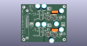
PCM63 JLSounds on top, Miro 1 PSU, LT1354 output.
Wonderful!

Wonderful!
@Tea-Bag , this is correct.I am not sure what pins go where for Miro's 4,2...
Does the 11->4, and 15-2?
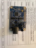
Do you mind showing a picture of your JLSounds board?
@Tea-BagI wish to just do thse two things, and assume that jumpering the JLSounds board per screenshot will work H1.1->H3.17, H1.2->H3.19.
1. I assume this is just for initial testing only? It is better to eventually have their separate individual supplies
2. Have you soldered the smd shift register ICs? Since you have the JLSounds board, you can actually skip them.
However if you insist on the i2s format source, the shift registers must be used and please use the following configuration, assuming that your JLSounds board is VIII (not the FIO version) :
So you need to remove jumper 4 from your board.....
A picture of your JLSounds board will be good for verification of the version you have.
@Tea-Bag
My recommendation is for you to skip the shift registers and connect the JLSounds signals directly to the AD1862.

To enable the JLSounds to do this , follow this configuration :

My recommendation is for you to skip the shift registers and connect the JLSounds signals directly to the AD1862.
To enable the JLSounds to do this , follow this configuration :
Cut open JP1 and JP2. DNP J9 (this will remove the +5VD routing to the shift register ICs)
And of course DNP IC1 ~ IC6 and C1 ~ C6.


JLS 9 -> DAC DR
JLS BCLK -> DAC pin 4 i2s input
JLS 13 -> DAC DL
JLS 15 -> DAC pin 2 i2s input
JLS 2-16 -> DAC Gnd at i2s input
(any one)
And of course DNP IC1 ~ IC6 and C1 ~ C6.
JLS 9 -> DAC DR
JLS BCLK -> DAC pin 4 i2s input
JLS 13 -> DAC DL
JLS 15 -> DAC pin 2 i2s input
JLS 2-16 -> DAC Gnd at i2s input
(any one)
Last edited:
Thanks for looking at this. I have been offered a board by another member that mounts jlsounds on top of it. It will likely be less complicated for me.
Here is the jlsounds board. The plan is to make a seperate 5v supply for jlsounds board after making sure I can get it working with basic supply first. New dac board will be the following design, and looks to be copy of one I heard earlier this year and enjoyed a lot.
Here is the jlsounds board. The plan is to make a seperate 5v supply for jlsounds board after making sure I can get it working with basic supply first. New dac board will be the following design, and looks to be copy of one I heard earlier this year and enjoyed a lot.
Attachments
This is my SPDIF input board, using AK4118 as receiver.@Tea-Bag , this is correct.
Do you mind showing a picture of your JLSounds board?
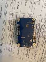
This is a modular test board. It is used for my various DAC tests.
Or do you have a better suggestion?
- Home
- Source & Line
- Digital Line Level
- DAC AD1862: Almost THT, I2S input, NOS, R-2R