

 Certainly dead, but you can try in I2S mode (pin 27 to 26) with pin 4 floating or grounded (should be grounded though in I2S mode). IIRC input pins have diode protections but not sure it resist to -15V ! It has probably made a short wuth the positive voltage of the pin 4 if it was tied to the front end !
Check also the front end (JLS, or CPLD or shift register according what frontend you have).
I re read Plato and he said that only people never soldering never break IC !

Is it not necessary for pin4 to be fed Bit Clock when one configures the TDA1541 in i2s mode?
I maybe mix the pins position. The idea is : 5Vpin to pin 27 = I2S mode & -5V pin to pin 27 is simultaneous mode.
Pin 4 is data R and shorted to Pin 5 Agnd in I2S mode in datasheets. I will works too grounded to Dgnd or to Sclk pin but doesn't need it, So assume than floating is feasible to in case of short of the input without deep damage inside ? The Wclk pin 1 is not latched in I2S mode and it manages the Data L/R multiplexing on pin 3 as it works in word clock mode. (pind +5V to pin 27)
// cap pin 16 to 17 not populated with non-A TDA1541 (the cap is inside). Maybe yes it needs with non A to toed pin 4 to 3 (don't remember it all)
Last edited:
TDA1541A : If some want a 4 layers efficient smd board with the classic datasheet grounding and with just uf-l I2S/Sim and a raw for JLsounds board, tell me or make an interrested GB, should be less than 30 euros for 4 layers w/o shippment & w/o I/V stage. (and will be better than all the faux solded kits seen here and there but Audial's or Thorsten's).
Last edited:
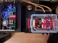
Take into account that powering with a 12V voltage on the +-5V side may cause the stabilizers to heat up more, as they have a greater voltage difference.I don't know where my idea came from to order a transformer with 2x5VAC and 2x 12VAC outputs. PSU No. 2 needs only 2x12.
There is not much heating there, the currents are quite low. The heating of the heatsink is hardly noticeable, I even think that everything can work without any heatsink, but I put them on anyway, they are cheap.
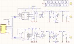
The one thing I missed in Miro's boards is the reconstruction filter so I decided to make a PCB with one (WIP):

4 layer board, going to pair it with the PSU posted earlier. Main question is the input, since I want to have both USB (York) and Bluetooth options (Bluetooth would require resampling), I am going to separate all of that and and just have clocks + reclock register on the DAC board.
(Don't pay attention to values on the schematic, they are all wrong 🙂 )
Attachments

Made that a lot , souvent du Bordeaux or du Bourgone but as well as Anjou or Alsace or Languedoc ! In pack of three or six wine bottles they are handy for diy !
Problem is the spouse ! : "Darling,, are you making a bomb, should I call the police ?" 😱

Problem is the spouse ! : "Darling,, are you making a bomb, should I call the police ?" 😱
I am experimenting with LED bias for tubes (again). I like the result. Now I'm waiting for the IR diodes to arrive. That should be even better.happy the plastic cases are back, I missed them ! 😍
less noiser with the IR but you need a lot. Resistor is just perfect bias but if you use microphonic tube or DHT ones ?! 🤔
RCA 5670 & TESLA 6CC42
No microphonics in this plastic case either.
No microphonics in this plastic case either.
So this will be an AD1862 board with output filters? Or do I misunderstand?The one thing I missed in Miro's boards is the reconstruction filter so I decided to make a PCB with one (WIP):
4 layer board, going to pair it with the PSU posted earlier. Main question is the input, since I want to have both USB (York) and Bluetooth options (Bluetooth would require resampling), I am going to separate all of that and and just have clocks + reclock register on the DAC board.
(Don't pay attention to values on the schematic, they are all wrong 🙂 )
It's an Aikido preamp. A Chinese version with 6N3 tubes that I converted into something useful a long time ago. With LED bias voltage gain is high (36×). The solution is NFB for gain 3x.@NIXIE62 schematic for that stage?
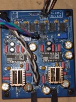
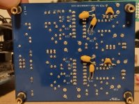
Yes, that's correctSo this will be an AD1862 board with output filters?
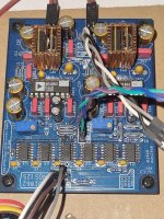
Hello everyone, some time ago I bought a used Ad1862 dac. Could someone check if all the elements are ok? It sounds nice, but the stage width and some bass attack are missing. I am not an electronics guy, more of a hobbyist.
Attachments

- Home
- Source & Line
- Digital Line Level
- DAC AD1862: Almost THT, I2S input, NOS, R-2R