
Do I understand correctly that using PSU 1 or 2 there will be no problem with connecting AGND and DGND in the wrong place?
A Layout PDF attached.That is the case in fact, I mentioned earlier that two sections of the PSU have separate grounds. So the agnd and dgnd are connected on the DAC board.
Attachments
That's funny I am not trusted after 5 pcb design of an AD1862 made for high frequencies op amps, ahaha ! Thanks miro1360 ! Yes the purpose of that is the 2 pins must be connected, the lowest distance and cleanest path together ! The cleanest though is almost a joke and ask some creativity for playing with the 4 layers ! It's a little a current washing machine bellow the chip, mixing the dirt cloth with the less dirt ones.
I would say it 's essential to connect them near these 2 pins only, under the chips bully, somewhat but digital line and power supplies make the things not easy, as the fact there are two chips.
No probs Eclipsevl, we didn't understand you was talking about the power supply pcb and not the DAC one. Pcb are expensive 😉
Last edited:
Oh no, don't take it personal. It was just the language barrier 🙂That's funny I am not trusted after 5 pcb design of an AD1862 made for high frequencies op amps, ahaha !
I said it second degree ! 🙂 (you know, my rock'n roll famous gale attitude !)
Btw I didn't finished to test the AD811, but fuses arrived today, I have somewhere a short that burn the positive fuse on the PSU2 (I removed one LT1963 and it is not the culpritt, I am to check the diode bridge now but I'd better construct another PSUII as I have all the parts !
I am slower and slower...
Last edited:
These PSU are designed to work with my DACs, but you can use it for another projects as well. Grounds are connected on filtration capacitors, then separated at the regulators and then it depends on the application where they will be connected (for DACs they should be connected near the DAC chips - on the DAC pcb) 🙂Do I understand correctly that using PSU 1 or 2 there will be no problem with connecting AGND and DGND in the wrong place?
Did couple of measurements today, PCM63 DAC at 0dB:

-100dB @ 50Hz, I think is a decent result for DAC on a cardboard 🙂
-100dB @ 50Hz, I think is a decent result for DAC on a cardboard 🙂
Last edited:
I removed the trimming circuits and tantalums C31 and C36 and it seems to be better 🙂@Tommar
1. Jaki jest wzmacniacz uruchamiający I/V w grzejnikach? Może zmień idź na coś innego. Lubię LM6171, ale możesz też spróbować OPA1655.
2. Odlutuj TR1, TR2, R4, R5, R6, R7...
3. Odlutuj C31, C36
4. Jaki jest rezystor I/V? Można, że wartość otrzymana z I/V. R8, R9: wydanie z I/V (L-OUT, R-OUT), 1k4==1,4Vp, 2k4==2,4Vp, 2k7==2,7Vp (2,7Vp==5,4Vp-p)
5. C15, C16, C25, C26: należy zwrócić uwagę na wartości (stosunek 1:10), należy zwrócić uwagę na elektrolit wysokiej jakości (teraz jest to tantal) ... wartości takie jak 4u7 + 47u lub 10u + 100u
:Fajny:
sprawdź również, czy oba urządzenia brzmią tak samo, znajdują się w różnych układach scalone (mogą pochodzić z innych urządzeń z eBay'a, których informacje są w porządku, ale muszą być wymagane)
I have a few more questions:
1. I don't know how to check if both circuits play the same. I have an oscilloscope and a Focusrite interface. Is there a way to test this?
2. Is it possible to trim the chips correctly using the linearity test from post #33?
3. Is it better to order new chips with the same numbers instead?
4. Is it worth replacing any other elements with better ones?
5. Is it worth making @Hidy's modification from post #2687 for Burson v7 classic? I assume that it is possible to continue testing other operational amplifiers, e.g. sparkos or staccato.
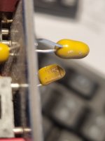
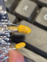
6. @Brijac Capacitors C25, C26, C15, C16 are probably for C26 and C16 2x10uF (one on the top of the board and the other on the bottom) and for C15 and C16 2x1uF (one on the top of the board and the other on the bottom). Please verify because I'm not sure if I'm reading the values correctly. I'm uploading photos to check.
7. Is it better to put 4.7uF and 47uF or 10uF and 100uF in these places? What's the difference?
8. What wiring should I use for i2s connections, and what for the power supply?
Attachments
On the BOM from the first post the value for R10/11 should be between 22-100 ohm.
How do you choose the size?
I see many boards but none have the MSB components
Any reason why?
And if you populate the board, how do you make the adjustment?
How do you choose the size?
I see many boards but none have the MSB components
Any reason why?
And if you populate the board, how do you make the adjustment?
I know that the thread has answers to some or all of my questions, but finding them is like traveling around the world 😁 Besides, there are different opinions. I am also a beginner hobbyist, so many things are still incomprehensible to me.
@Cauwil what are these R10, R11 for? Does their quality affect the sound?
@diyiggy there are many answers there, but I would also like to understand how it works and why this particular element and not another 🙂
@Cauwil what are these R10, R11 for? Does their quality affect the sound?
@diyiggy there are many answers there, but I would also like to understand how it works and why this particular element and not another 🙂
@zoom777 You wrote that Nichicon KZ are unavailable. They are available on my local auction site. I thought I would order Nichicon Muse KZ 10u/100v UKZ2A101MHM1TN and 100u/100v UKZ2A101MHM1TN. I chose 100v because someone in the thread wrote that higher voltage means lower ESR, I think... They are big but I will fit somehow. Will this be a better choice than Panasonic?
They are physically huge, with thicker legs. If you think you can fit it on the board, I would subjectively think they are better than the Panasonic caps in this application.
Edit to add: as you have mentioned, there are different opinions for selection of parts. Some said tantalum is better than electrolytic caps just on the previous page, while I recommend otherwise. Some may favour certain caps over another.
Edit to add: as you have mentioned, there are different opinions for selection of parts. Some said tantalum is better than electrolytic caps just on the previous page, while I recommend otherwise. Some may favour certain caps over another.
Last edited:
Tommar,
Check out the AD1862 Datasheet.
The caps installed for NR1 and NR2 do not need to be 10uF and 100uF, Miro’s choice of 4u7 and 47uF is more than sufficient. The 100V KZ caps are way to big for the pcb. There are many different builds with just as many different cap combinations in this thread. There is no ‘best’ answer, you’re going to have to experiment.
BTW, I’ve had great listening results using regular ol’Tants in the noise reduction positions🤫.
If you don’t have the equipment to properly adjust the MSB, better leaving the components unpopulated.
- Home
- Source & Line
- Digital Line Level
- DAC AD1862: Almost THT, I2S input, NOS, R-2R