That's the idea - once the schematic is correct, and you've defined all the part footprints that you need, then you go on to the pcb drawing / routeing stage - that'll be the most time consuming. You can obviously still make changes to parts etc. while working on the pcb, but it becomes slightly more involved; all the part footprints you've selected now become scaled 'objects' on the pcb.
I tend to start just by setting up the basic area of the pcb (ca. 50 x 50 mm in the case), then you see directly the 'space' you're working to. Beyond that, I'm only now getting started with routeing SMD parts, so... 🤞
I tend to start just by setting up the basic area of the pcb (ca. 50 x 50 mm in the case), then you see directly the 'space' you're working to. Beyond that, I'm only now getting started with routeing SMD parts, so... 🤞

A bit more of the practical bit,
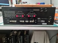
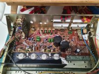
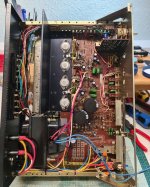
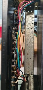
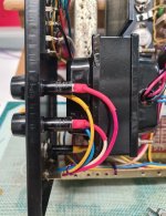
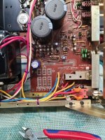
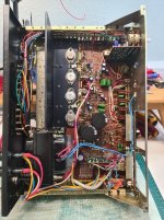
Most of the wiring in now and i will take it to the point of powering up today and ill finish now before moving on and concentratiing on finishing the PCB
Most of the wiring in now and i will take it to the point of powering up today and ill finish now before moving on and concentratiing on finishing the PCB
Attachments
It'll fit, but you do need to choose appropriate component sizes & orientations, e.g., electro cap. diameters, ceramic cap dimensions, resistor sizes (and vert. or horiz.), and so on - refer to the photos I posted previously for resistor vert./horiz. and approx. component dimensions. As an example: for an electro cap, I use Mouser to select the uF & voltage needed, and then check the actual part dimensions shown for the various results Mouser gives - before actually selecting which part I want to use, e.g., a 6mm or 8mm part, etc. The datasheets for virtually every part in the Mouser catalogue gives exact part dimensions. This is where the importance of the part 'footprints' chosen becomes paramount... especially if you're working to a fixed pcb size.
You can edit footprints using either the 'assign footprints' tool on the schematic sheet, or directly on the pcb layout sheet (right click any part, and it's an option). You will need to keep track so that changes on the schematic sheet and on the pcb sheet remain consistent with each other, so look for the buttons to 'update' the schematic from part changes you make on the pcb, and the other button to 'update' the pcb from changes on the schematic sheet.
I've been through part of the exercise for discrete components, and would strongly recommend to at least start with the NAD pcb layout you posted previously (from the manual) - try dropping the transistors onto the pcb in approx. the right place (and orientation), and work from there.
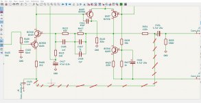
I did do that with the capacitors,and these are actual size as fitted,which is why I wondered if I had done the board the right size/way. I did watch videos of how to do it so it should be right,but looks out of proportion
SMDs can go on both sides of the board. Four layer boards are cheap. Density problem solved, I think.
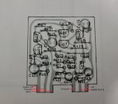
I see what you mean.when you look at it in the 3D model, it looks okIt'll fit, but you do need to choose appropriate component sizes & orientations, e.g., electro cap. diameters, ceramic cap dimensions, resistor sizes (and vert. or horiz.), and so on - refer to the photos I posted previously for resistor vert./horiz. and approx. component dimensions. As an example: for an electro cap, I use Mouser to select the uF & voltage needed, and then check the actual part dimensions shown for the various results Mouser gives - before actually selecting which part I want to use, e.g., a 6mm or 8mm part, etc. The datasheets for virtually every part in the Mouser catalogue gives exact part dimensions. This is where the importance of the part 'footprints' chosen becomes paramount... especially if you're working to a fixed pcb size.
You can edit footprints using either the 'assign footprints' tool on the schematic sheet, or directly on the pcb layout sheet (right click any part, and it's an option). You will need to keep track so that changes on the schematic sheet and on the pcb sheet remain consistent with each other, so look for the buttons to 'update' the schematic from part changes you make on the pcb, and the other button to 'update' the pcb from changes on the schematic sheet.
I've been through part of the exercise for discrete components, and would strongly recommend to at least start with the NAD pcb layout you posted previously (from the manual) - try dropping the transistors onto the pcb in approx. the right place (and orientation), and work from there.
I did do that with the capacitors,and these are actual size as fitted,which is why I wondered if I had done the board the right size/way. I did watch videos of how to do it so it should be right,but looks out of proportion
The largest electrolytic on the original pcb in my NAD 3030 is ca. 5mm diam., possibly 6.3mm, but certainly not >10mm. Your SMD caps inside the board outline above look to be >10mm square - so I'm not sure what you mean by "these are actual size as fitted" ? Are you aiming to build the board using smd parts or thru' hole ?
Can you post a screenshot of your 'footprint assignment tool' page (the one showing all the footprints being used on one page) ? I can't see the part sizes you're using from the screenshot above. I can see that you have only one vertical resistor footrpint assigned - check the manual drawing & my pcb photos and you should see it uses ca. 10 vertical resistors, all of which take up much less space (which I suspect is why NAD put them vertical - it's not for heat dissipation in a phono stage... it's probably only space-saving).
I wouldn't focus too heavily on the 3D viewer at this stage... you'll find it very useful for examining everything overall, and esp. the silkscreen and front fabrication layers, but it doesn't help much if at all while laying the board out / routing the tracks.
they are all intended to be standard through hole.but all have SMD referenceThe largest electrolytic on the original pcb in my NAD 3030 is ca. 5mm diam., possibly 6.3mm, but certainly not >10mm. Your SMD caps inside the board outline above look to be >10mm square - so I'm not sure what you mean by "these are actual size as fitted" ? Are you aiming to build the board using smd parts or thru' hole ?
Can you post a screenshot of your 'footprint assignment tool' page (the one showing all the footprints being used on one page) ? I can't see the part sizes you're using from the screenshot above. I can see that you have only one vertical resistor footrpint assigned - check the manual drawing & my pcb photos and you should see it uses ca. 10 vertical resistors, all of which take up much less space (which I suspect is why NAD put them vertical - it's not for heat dissipation in a phono stage... it's probably only space-saving).
i cant find any that dont say SMD
so im doing ok here but a couple of things i cant work outI wouldn't focus too heavily on the 3D viewer at this stage... you'll find it very useful for examining everything overall, and esp. the silkscreen and front fabrication layers, but it doesn't help much if at all while laying the board out / routing the tracks.
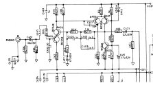
C426, i cannot find on the scheme at all, bit wierd, or im blind.
Im missing C418, so i can add that
I also need the 6th pin for the other ground, so i should be able to add that
# C425 & C426 are the 1nf ceramic caps on the rear of the phono input sockets - they're not on the phono pcb's. C426 in any case is an 'even' number, so shouldn't be in this channel anyway (all the 'odd' part numbers...). You probably put C426 into the schematic when you were starting, and it got carried over onto the pcb layout (& 3D viewer). At some point after that, you must have deleted it from the schematic, but not 'updated' the pcb layout for changes made to the schematic - so it stayed on the pcb layout. Remember you need to keep the 'schematic information' sychronised with the 'pcb layout information' - changes to one don't necessarily dynamically update to the other (there are contextual buttons on the top menus in Kicad to update one from the other, and vice versa).
Another way to 'find' something like this - is to leave the 'Ratsnest' visible - then you see from the white lines exactly how any part connects into the rest of the circuit. The Ratsnest will become your best friend... I would guess in this case, if you turn it on, C426 will show no connections to anything at all.
# C418 - another 'even' number ? I'd guess it's missing because it's supposed to be missing. Note: there is a slight mistake / inconsistency in the original NAD numbering, with C423 - C426. I'd just keep the odd numbers for this channel.
# Parts layout on the board looks ok for now (vs. the originals). You can just 'put' the J1 to J6 connectors off the bottom of the board for now. If you use the original NAD connection method, you'll need to add the two small board 'extensions' later, where the connections will be made. I'd also aim to try and keep the components all as 'high' up the board as possible. It'll only be a few mm but it'll help prevent 'fouling' of other parts on the main pcb (you can see the available space better than I can, in your rebuilt amp).
# It'll help if you 'label' the Input, Output, and PS 'Nets' on the schematic, one Ground is already done - and I also noticed 2x errors on the schematic, check around your -ve PS rail, and the amp output areas. They need to be corrected before you start laying out pcb tracks, or the errors transfer to the pcb as well.
@Goldie99
so the question is what one do i trust
the scheme,or the PCB layout?
cap line 1 is the scheme section
cap line is how it is shown on the pcb-i have striked the line out
so the question is what one do i trust
the scheme,or the PCB layout?
cap line 1 is the scheme section
cap line is how it is shown on the pcb-i have striked the line out
Attachments
- Home
- Amplifiers
- Solid State
- NAD 3030 complete rebuild