ill PM you the filesHi Poundy
Great to see you bringing life back to a NAD 3030. I'm sure it will be sounding fine, and be HiFi and maybe not High End 🙂
I have bden the happy owner of a NAD 3020 bought after my confirmation 🙂
Keep it original, don't change the output transistors. Newer types will have other characteristics, and you will have to at least ensure no oscillation and other ill effects.
For the phono amp, have you considered using SMD components? You can have JLCPCB mount most at very little extra cost.
If you share the KiCad files I can help you. You need to find out how the PCB outline should be, and as Goldie99 says ensure the right pin put so that it fits down in the main pcb.
As Goldie99 says you should define the connector row (pin row) that you will connect all in, out and power to, that will be the interface to the main board.
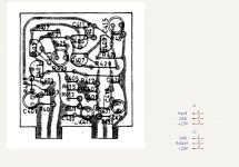
Can you also share the original phono schematics in order to check?
Go for it
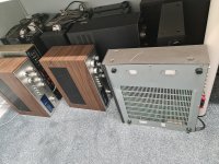
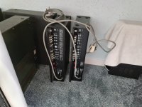
I also have this lot to deal with yet as well.
Attachments

You need to go through each in turn, but at first glance:
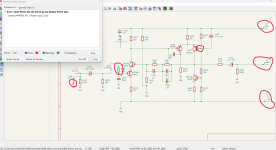
1) You've put a connector onto the signal +ve input (J1 - looks good), but you don't have any signal -ve input at all
2) J2, J3, J4 are not connected to the schematic at all - you need to flip them around and connect the schematic traces to then - zoom in on J2, J3, J4 and the little red arrows are pointing at the problem.
3) You have 3 different grounds in there - zoom in on each of the "GND" connections and make sure they're connected properly, you also have a "GND?" label up by C423 that I assume is a typo, and you have a "GNDPWR" Earth symbol just floating about not connected to anything (delete that). You can split the signal grounds out - just call them GND1 (at R401, R403, and C403)
4) You've also got errors in the schematic still, e.g., J4 - once it's connected to the trace, will also be directly connected to GND... (you're missing a decoupling cap on the schematic I think). There should probably also be a cap below C413 as well ? I haven't checked the rest...
Ok thanks,ill check them shortlyYou need to go through each in turn, but at first glance:
1) You've put a connector onto the signal +ve input (J1 - looks good), but you don't have any signal -ve input at all
2) J2, J3, J4 are not connected to the schematic at all - you need to flip them around and connect the schematic traces to then - zoom in on J2, J3, J4 and the little red arrows are pointing at the problem.
3) You have 3 different grounds in there - zoom in on each of the "GND" connections and make sure they're connected properly, you also have a "GND?" label up by C423 that I assume is a typo, and you have a "GNDPWR" Earth symbol just floating about not connected to anything (delete that). You can split the signal grounds out - just call them GND1 (at R401, R403, and C403)
4) You've also got errors in the schematic still, e.g., J4 - once it's connected to the trace, will also be directly connected to GND... (you're missing a decoupling cap on the schematic I think). There should probably also be a cap below C413 as well ? I haven't checked the rest...
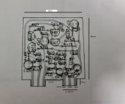
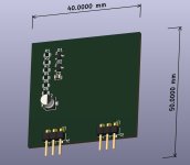
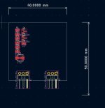
I would make the 2 x 3 pin out like this. Then it is easy to design an place on the pcb.
Excellent approach - forcing the pcb track & connection geometry by virtue of the connector, I like it.
Here is a starting point.
You of course need to change a lot
I think I got the pin order correct, but check it twice at least 🙂
Also schematics need to be checked a lot.
Use E.g. BC856 instead of mmbt5401 etc. Change the JLCPCB numbers for each component (double click on each component), and also change the component values
Define the pcb layout by changing / adding cut out lines .... I have just made a square one
You need to measure the pin distance .... probably not the 2.54 mm I have used ... you could change to single pins and distance them correctly
Install the JLCPCB Fabrication Toolkit plugin in KiCad, then you make all the fabrication files by one click of a button 😉
I would use a double layer pcb as it is of zero extra cost, and place GND on that (I have added it to bottom layer ... blue)
Attachments
so i just have the one isse here on screen, but one arrow, not connected to the fault it is showing up.I dont understand why that arrow is there, ive tried everything,the symbol,making sure its connected etcYou need to go through each in turn, but at first glance:
1) You've put a connector onto the signal +ve input (J1 - looks good), but you don't have any signal -ve input at all
2) J2, J3, J4 are not connected to the schematic at all - you need to flip them around and connect the schematic traces to then - zoom in on J2, J3, J4 and the little red arrows are pointing at the problem.
3) You have 3 different grounds in there - zoom in on each of the "GND" connections and make sure they're connected properly, you also have a "GND?" label up by C423 that I assume is a typo, and you have a "GNDPWR" Earth symbol just floating about not connected to anything (delete that). You can split the signal grounds out - just call them GND1 (at R401, R403, and C403)
4) You've also got errors in the schematic still, e.g., J4 - once it's connected to the trace, will also be directly connected to GND... (you're missing a decoupling cap on the schematic I think). There should probably also be a cap below C413 as well ? I haven't checked the rest...
Im nearly there with it.
As Baldin says... there's plenty of errors on the schematic - Kicad can only check that it's 'electrical rules' are correct, not if the schematic itself is.
R411 value 10m ?
Missing cap on -ve rail ? so J4 shorts to GND
Missing cap between R411/R413 to GND ?
R411 value 10m ?
Missing cap on -ve rail ? so J4 shorts to GND
Missing cap between R411/R413 to GND ?
Hi Baldin - I did take a quick look. It looks like a good basis for an SMD board, albeit possibly a nightmare for routeing (?), but I had to install Kicad 8 to open the files.... and I somehow managed to lose a Kicad 6 project I'd been working on (and almost finished), so I'm currently running a 'restore' from back-up, hoping I'll be able to recover it. Not at all sure at this point, but my mistake, so ... we'll see.Did you try my files?
this should be better, but i just cant get rid of the arrow on the groundThink there are more than one error ..... take a look at these places ... R405 shorted, Q407 base not connected, +,- and out connected but overwritten, same as for GND on C426
Attachments
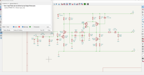
Forget the red arrow until you have the basics right - as it is now, you have one voltage rail shorted to ground, and the other connected via 10 milliohms to ground... correct the schematic and most if not all will drop into place.
Wow, I didn't know NAD made stuff before the 3020, in my childhool the 3020 appeared as if by magic!I also have this lot to deal with yet as well.
I note that they have power meters, this is an excellent sign: very cool!
Ahhh sorry to hear that🙁 ..... Are you really sure it is lost ... can't you find the files directly where they are stored on the PC?Hi Baldin - I did take a quick look. It looks like a good basis for an SMD board, albeit possibly a nightmare for routeing (?), but I had to install Kicad 8 to open the files.... and I somehow managed to lose a Kicad 6 project I'd been working on (and almost finished), so I'm currently running a 'restore' from back-up, hoping I'll be able to recover it. Not at all sure at this point, but my mistake, so ... we'll see.
PS. SMDs are not at all that difficult to route, and it makes it possible for JLCBPC or other manufacture to mount most of the components. I usually get all the basics mount and then I only have to mount through hole and components which JLCPBC do not stock.
Also 4 layer has become so cheap that this is my default now. 10x10 cm for 7 usd !!!
- Home
- Amplifiers
- Solid State
- NAD 3030 complete rebuild