Excellent work @Icsazcar.
With tda15xx chips I noticed that:
Best results:
DEM oscillator & FSYNC injection locks, causing bursts of flank displacement on Fsync => 👎 (Tek 500 Mhz oscill + Micro display)
I think someone mentioned this - John? Thorsten?
This might differ on different chips.
I used old chip from 1987.
Grundig/HtP solution of externally driven dem + reclock reduced the problem. Recommended.
Cheers
With tda15xx chips I noticed that:
- type of caps
- their physical dimensions/construction
Best results:
- wide smd's > 100 nF
- inwards, underneath the chip
- onto a solid gnd plane.
DEM oscillator & FSYNC injection locks, causing bursts of flank displacement on Fsync => 👎 (Tek 500 Mhz oscill + Micro display)
I think someone mentioned this - John? Thorsten?
This might differ on different chips.
I used old chip from 1987.
Grundig/HtP solution of externally driven dem + reclock reduced the problem. Recommended.
Cheers
Last edited:
Now I measured the -3 dB cutoff frequency of each decoupling internal R and external C (100 nF). Here are the measured values:
To be clear, the cap in the picture is the only cap in circuit for this pin and you send in a low impedance, low level sine wave and measure the voltage at the pin for a 3dB cutoff?
Bit 9: 175 Hz
Bit 10: 170 Hz
Bit 11: 370 Hz
Bit 12: 235 Hz
Bit 13: 360 Hz
Bit 14: 360 Hz
Bit 15: 800 Hz
The calculated internal resistances are:
Pin 24, 7: 9.1k
Pin 23, 8: 9.4k
Pin 22, 9: 4.3k
Pin 21, 10: 6.8k
Pin 20, 11: 4.4k
Pin 19, 12: 4.4k
Pin 18, 13: 2.0 k
Excellent work. Seeing how hard resistors on chip were in those days (much harder than a diode or NPN Transistor) and the likelyhood of +/-50% worst case tolerance (IIRC) I suspect the "nominal" values are something like:
LSB to MSB
9k/9k/4k5/4k5/4k5/4k5/2k25
This is a heavy guess,
DEM decoupling capacitor sizing
Based on the measured internal resistances of the DEM pins and Thor's excellent explanation here
https://www.diyaudio.com/community/...ac-using-tda1541a.79452/page-495#post-7820751
I recommend the following capacitor values:
Pin 24, 7: 100 nF
Pin 23, 8: 100 nF
Pin 22, 9: 100 nF
Pin 21, 10: 120 nF (100 nF should be OK)
Pin 20, 11: 100 nF
Pin 19, 12: 220 nF
Pin 18, 13: 220 nF
The values are for ~180 kHz DEM frequency. They are a function of internal resistance and ripple frequency (fDEM/2 or fDEM/4). Half internal resistance needs double capacitance, and double frequency (fDEM/2 vs. fDEM/4) needs half capacitance. This wiil give about 48 dB attenuation of ripple.
That's only partially correct.
The current ripple at each pin is a percentage of the pin's reference current. This enters into the calculation. Here a quick spreadsheet I did:
Now this is is a "worst case" calculation based on RJvdP's article. The 4-Way transistor current splitter is described as "better than 5% tolerance".
So I calculate with 5% of the pin's reference current as peak-peak ripple. This current will primarily flow in the DEM filter cap, as it at least 100 times lower impedance than the pin input resistance. I could have made the calculations more complex accounting for the pin resistance, but I decided that error from ignoring this is not material in context.
The actual current ripple will vary from IC to IC and from pin group to pin group and is likely materially lower than what my calculations show.
This also does not account of the integrating effect of the first order filter typically applied in the I/U Conversion or the 10n "RF loop" capacitors I recommend on ALO/AOR pin's. All these will reduce error within the audio band.
Still, the worst case ripple on MSB is way past 1/2 MSB if we use 100nF.
Note, if measuring using any system that uses averaging, be it FFT with a meaningful Window or integrating HD meters etc. will average out the ripple and it will not show in the measurement.
Human hearing is also an integrator for pure tones. Is that enough?
Anyway, all steady state measurements will average out this ripple, but it still exists.
Now, we have a few possible mitigation strategies.
If we make sure that the DEM frequency is an integer multiple 4 X Fs - each sample receives all four currents of the current splitter - and so integrated over one sample, the current ripple becomes zero. With further integration in the I/U conversion the ripple averages out.
Another mitigation strategy is to increase the filter capacitor values:
I think combining increased value DEM Filter Capacitors at the MSB's with FDEM = Integer Multiple of 4FS will push the problems below anything that matters. As there is little extra cost of effort it would seem a little foolish not to do this.
Thor
Silly question, you gents are now working on getting the optimum cap values for the Dem pins
Not really "Optimum" but rather minimum value to guarantee certain results under worst case conditions.
so what was John's idea of recommending the use of 100uf caps to slow down Dem if I recall correctly.
Another way. After looking carefully I decided that this is a bit too much dependent on parameters we cannot sufficiently control in the real world and long term, to recommend it.
What would the difference be when compared to using optimized cap values for each pin
Using very large capacitance values means capacitors need selecting for < 1/2 LSB current leakage under all possible operating conditions (temperature winter vs summer etc) and long term stable.
If this is done, we can afford to lower FDEM to values where the DEM ripple is at very low frequencies.
It means that the frequency (FDEM) with which the ~ 20nS glitches on the DEM Filter pins occur is much reduced over (say) 176.4khz.
At the same time the ability of the capacitors used to sink these glitches and avoid them entering the audio path is reduced.
So I expect that there will be subtle sonic differences.
But honestly I have no trust in the long term, stability of electrochemical condensers. 1Month? Sure. 1 Year, likely. 10 Years, yeah not happening.
Now C0G Ceramic or SMD Film condensers will still be 100% on spec in 10 years after much worse abuse the the electrochemical condensers.
So I decided against low frequency DEM after extensive consideration and instead prefer to focus on minimising problems from using 4 X FS DEM.
Speaking of Focus....
Thor


It's possible to have a workaround electrolitics for 50hz dem mod by using stacked 22uf smd pmlcaps. One big downside, it gets very expensive 🙂 But it has better esr and lower leakage, on top of lasting forever. Type of solution where you throw $ at it.
Current development is going to bridge the gap where 100hz dem mod had larger upper hand comparing what was known at the time. It's going to be better to invest into two tda1541a chips for less money, rather than that route and go Ascendance route.
Current development is going to bridge the gap where 100hz dem mod had larger upper hand comparing what was known at the time. It's going to be better to invest into two tda1541a chips for less money, rather than that route and go Ascendance route.
It's possible to have a workaround electrolitics for 50hz dem mod by using stacked 22uf smd pmlcaps. One big downside, it gets very expensive
Well, you need 100uF on several pins and way more on MSB's.
So until we get 100uF film in 1210 it's pretty much no go.
Thor
Yep. Cost is too large. As the project is right now, it's better to purchase two tda1541a chips and go Ascendance build.
the difference is so subttle between 100 uF solution and 1 uf solution, than I surmise the standalone TDA1541A migth better if you have a standalone 1998 Taiwan or S1/S2 than two normal 1988 TDA1541A . The FDEM decoupling is not the alpha and omega of a good sounding TDA 1541A, it is just we are focused on that at the moment, but IME, it is low in the list of what makes this chip sounding good.
YMMV, and some have two S2 Taiwann, ahaha ! And of course you never know before having listening to it 😉
YMMV, and some have two S2 Taiwann, ahaha ! And of course you never know before having listening to it 😉
Ok, looking around, I decided to make a few small changes to the design, here the single TDA1541 sensible "Core".

Key changes:
BC327 added to buffer the clock inputs of the 74F74, to avoid loading the clock. BC327 should be fine as follower at 50MHz. Internally each input is a Pin Diode (think 1N4148) and a 10k Pullup. So 4 clock inputs become a material load, we just don't want those currents to circulate across our input wiring. This way it's the base of a follower as load, with still decent beta at many MHz. Emitter load is ~ 2.5kOhm, base load less.
The attenuators and slew rate limiters are now "flying". This makes them a constant load regardless if Q or /Q are high (the other output is then low). This makes the 74F74 reclockers and signal conditioning mostly a constant load, if a chunky one at nearly 50mA. But they can now share the TDA1541 +5V and DGND with little issue.
So this overall simplifies things. DEM Clock is "Balanced Philips/Grundig" again with a flying balanced attenuator.
It may seem all a bit OTT and gilding the lily. Perhaps. I'm being quite minimalist by my standards.
I'm actually tempted to bring the MCK on board too, as the last element outside our control:

In a lot of ways what I propose is not miles off from Johns work around SD Trans with TDA1541 DAC era.
Thor
Key changes:
BC327 added to buffer the clock inputs of the 74F74, to avoid loading the clock. BC327 should be fine as follower at 50MHz. Internally each input is a Pin Diode (think 1N4148) and a 10k Pullup. So 4 clock inputs become a material load, we just don't want those currents to circulate across our input wiring. This way it's the base of a follower as load, with still decent beta at many MHz. Emitter load is ~ 2.5kOhm, base load less.
The attenuators and slew rate limiters are now "flying". This makes them a constant load regardless if Q or /Q are high (the other output is then low). This makes the 74F74 reclockers and signal conditioning mostly a constant load, if a chunky one at nearly 50mA. But they can now share the TDA1541 +5V and DGND with little issue.
So this overall simplifies things. DEM Clock is "Balanced Philips/Grundig" again with a flying balanced attenuator.
It may seem all a bit OTT and gilding the lily. Perhaps. I'm being quite minimalist by my standards.
I'm actually tempted to bring the MCK on board too, as the last element outside our control:
In a lot of ways what I propose is not miles off from Johns work around SD Trans with TDA1541 DAC era.
Thor
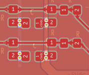
I spent dozen of hours to layout the previous attenuators nodes, lol ! (seepicture)


Okay, KISS is better 🙂 (less part less lipstick, pretier Lily, in France we prefer it white since the kings) .So all the attenuators caps and resistors shunt gone (no ropes nodes so flying), all the complex 0.1 uF between R shunted attenuators not needed anymore but at the power feet of the flip flops only (But EC1) rigth ?
No more Vcc_Gnd but DGND ground everywhere ?
Edit : BC327 quiet enough? Zetex instead or BC good enough ?
Attachments
Last edited:
Dummy's question : What the interest to embeding the MCLK if it must slave a distant USB/Spidf to I2S/SIM streamer ? Or writed differently : is jitter important enough for a pcm chip to make a complex circuit to reclock all near the TDA front end input before the attenuator to re inject it there ? Anyway there will be the jitter of the cpld itself if not all is reclocked after it ?
IIf wee lokk for instance at @Markw4 work to slave a JLSOUNDS USB or other frontend with his MCLK board + aside reclocker : should it be not good enough just aside the core board like that from MakW4 : https://www.diyaudio.com/community/threads/general-purpose-dac-clock-board.413001/post-7688633
IIf wee lokk for instance at @Markw4 work to slave a JLSOUNDS USB or other frontend with his MCLK board + aside reclocker : should it be not good enough just aside the core board like that from MakW4 : https://www.diyaudio.com/community/threads/general-purpose-dac-clock-board.413001/post-7688633
Ultimately it must be experimented with in practice. For example, John Brown wrote here at a certain point that the master clock should be nowhere near the dac. He didn't elaborate on it.
(IIRC, he came to this conclusion a while after experimenting with the onboard master clocks.)
(IIRC, he came to this conclusion a while after experimenting with the onboard master clocks.)
You know the story of the Kangaroo and the humming-bird ?
I don't want a Deception PCB more as all that came before at diya with ego centered for many TDA1541A pcb makers (when sold) and stupid followers.
But T. is on the boat desk with some good people like Icsazar and Zoran mostly. I try to make a core for at least the heads here to see if what they measure and hear is worthing the hundred hours I spent to make an affordable pcb for the diy peeps here.
Last edited:
Nothing wrong with what you say, I still remember your advices about piggy back diodes to protect ad1862 outputs years ago 🙂 ! Do you remember the good advices of @marce about layouting too in @Painkiller thread ?!
When the shematic will be in a go phase we need a pcb to measure in reality (beyond the verroboard experiences), I'm stuck on that but maybe I am wrong ? I really wanted a 6 layers because I thougth despite costing a little more it is better on a decoupling side and signal integrity due to the complexity of numbers of caps here and decoupling on both side of he IC and PS aeras, all being far away. But I came back to 4 layers for cost managment reasons for the majority of people can spend less : it is literally a looooooot of more hours in front of my pcb cad to do so (despite the good advices behind 🙂 ) ! So don't get me wrong too 🙂 !
When the shematic will be in a go phase we need a pcb to measure in reality (beyond the verroboard experiences), I'm stuck on that but maybe I am wrong ? I really wanted a 6 layers because I thougth despite costing a little more it is better on a decoupling side and signal integrity due to the complexity of numbers of caps here and decoupling on both side of he IC and PS aeras, all being far away. But I came back to 4 layers for cost managment reasons for the majority of people can spend less : it is literally a looooooot of more hours in front of my pcb cad to do so (despite the good advices behind 🙂 ) ! So don't get me wrong too 🙂 !
Attachments

Last edited:
Table each 'leg' sitting in water bowl. Sambal, sambal and more sambal. Ichan Bilis, ochre, kangkong, small fresh water fish about width of palm which had unusually disproportionate size heads - were 'dried' with salt, and for some reason with maggots (left to roam free before preparation). Fresh water (pond) 'snapper' (Nangai?) fed Tapioca leaves. Caught with net and thumb through the 'eye' to 'kill'.Waaaa bahasa indonesia boleh juga ya mantap. Kudos
Wear feet covering, the worms will 'up through your skin'.
Walk down jalan kampung, my wife at the time with scissors and basket, philosophy = 'take what you need, it all grows'. I was the only 'orang putih', and I could have stayed there happily. Treks, waterfalls, dragon fly the size of tennis ball. Rivers. Huts. Long-houses.
Slippery when wet tiles, sharp edges, big barrels full of water for 'wash' and toilet 'flush', squat ceramics for the same and ... reverse cycle air con and internet flat screen TV inside the house 🙂
I know how to grow a pineapple plant - you cut the top off and stick it in the ground. She would carve the pineapple from its skin, you'd have to see it to believe the consistency and the 'lack of waste'.
Looking back, I cherish it. Share, not for ego so much (there is some), but with my life 'as boring as it is' - to shout "I did exist !!!!!" 🙂
Last edited:
No more Vcc_Gnd but DGND ground everywhere ?
Except where there is AGND. But as both eventually tie together, they can overlap.
Edit : BC327 quiet enough? Zetex instead or BC good enough ?
The issue here is more "speed" but not switching speed, as this is a Class A linear circuit.
AssUMing a 3.3V CMOS source, at 0V in (low) the emitter is at 0.65V so 1.34mA flow. With 3.3V current will be below 0.1mA. We need a transistor with the low parasitic and high Ft to squarely pass 50MHz (pun intended).
Noise barely enters.
Dummy's question : What the interest to embeding the MCLK if it must slave a distant USB/Spidf to I2S/SIM streamer ?
Placing it under our control. The whole work I have done, as well as @Zoran, @lcsaszar has been about getting control over what goes on and taking guesswork out of design.
Or writed differently : is jitter important enough for a pcm chip to make a complex circuit to reclock all near the TDA front end input before the attenuator to re inject it there ? Anyway there will be the jitter of the cpld itself if not all is reclocked after it ?
We re-clock before the Attenuator.
Ultimately it must be experimented with in practice. For example, John Brown wrote here at a certain point that the master clock should be nowhere near the dac. He didn't elaborate on it.
(IIRC, he came to this conclusion a while after experimenting with the onboard master clocks.)
It's a tradeoff. At the DAC there is more noise, though shielding is possible.
On his SDTRANS he had the clock on board with the DAC:
I think a PCB with at least a local discrete clock option embedded makes sure we are able to take control. I like John's clock above, we need of course 22.5792/24.576MHz and the ability to switch frequency and MMBF4393 instead of 2SK170 should be ok...
Thor
On his SDTRANS he had the clock on board with the DAC:
BTW, the power supply:
Thor
To Glock, or not to Glock? Is that the question here?
And do we use a standard Mag, 30 Round extended Mag or a 100 Round double drum Beta C-Mag for extra fun?

Ahhhm, wrong topic or forum.
To CLOCK.... Not Glock.
Why am mixing them up all the time? Must be because my watch making friend gave me a "b-Grade" Glock P80 watch... So I'm often wearing my Glock Clock....
So, embedded clock, with two gears. Maybe something like this? With a 100k resistor to -5V and a pair of PNP transistors (emitter of first one gets 3.3k, base to GND and collector to one node, second transistor inverts) to select the gear?

Needs breadboarding, next to impossible to simulate Glocks, I mean Clocks...
Thor
And do we use a standard Mag, 30 Round extended Mag or a 100 Round double drum Beta C-Mag for extra fun?
Ahhhm, wrong topic or forum.
To CLOCK.... Not Glock.
Why am mixing them up all the time? Must be because my watch making friend gave me a "b-Grade" Glock P80 watch... So I'm often wearing my Glock Clock....
So, embedded clock, with two gears. Maybe something like this? With a 100k resistor to -5V and a pair of PNP transistors (emitter of first one gets 3.3k, base to GND and collector to one node, second transistor inverts) to select the gear?
Needs breadboarding, next to impossible to simulate Glocks, I mean Clocks...
Thor
- Home
- Source & Line
- Digital Line Level
- Building the ultimate NOS DAC using TDA1541A