Thanks Thorsten for sharing.
I understood it all, with the exception of the JFET compounds. Could you explain them in detail? I don't get how they work.
(BTW I understand the BJT compound).
Thanks,
Alex
I understood it all, with the exception of the JFET compounds. Could you explain them in detail? I don't get how they work.
(BTW I understand the BJT compound).
Thanks,
Alex
Did You tried ES9008, first model? Current mode. Somehow I think that sounds better from all other ES. I dont know... I didnt compare directly... I used also 100MHz clock.IME the ES9018 sounds best in voltage mode
Understood bro what Im saying is whatever input impedance from input of trafo i/v stage the output impedance will be multiplied hence.This is the honnest assertion I was waiting ! 🙂
Tubes can be very linear too; wider as well ? In the Adagio DAC, T Loesch used both traffo elevation and tubes.
@sumotan , in our quest this is not the output impedance of theI/V stage that is a problem, it is still the input impedance the DAC sees at the I/V input! One wants a low impedance to ground. The dac it self has an output impedance, capacitance as well (if you want to calcualte find the closed loop of an active I/V stage with an op amp for instance...
In that regard I am not sure tubes or traffos have a palm between each others, They still are ruled by the I/V resistor and the too much high impedance seen ... . Curent conveyor can solve that, then use any Riv value you need after.
Then for the stages that follow till the amp, impedance adaptation between two stage with a ratio of 1/10 is fine, at least my understanding. Btw, I always found passive pre with traffo to lack of something and soundstage.
Edit : I gave above to Thosrten a link about a good active I/V discrete on the paper (just lack the curent injection of 2 mA to adapt to the tda1541A) made by Sergio and measured -130 dB by Bohrok member (sligthy modified with Jfet if I remember).
I hope Thorsten says more when people have dealt with a pcb proto or even before as this story of 5V ref is a part of it
The other issue is voltage gain with no current gain will never driver the music well, this I've proven to myself with lots of experiments.
Hi Thorsten do You know maybe what difference is allowed from DGND (pin 14) and AGND (pin 5) pins on TDA1541A?For -5V to +5V the 100n C0G + 680n ECPU is usable. Same for actual -15V to AGND decoupling.
Hi Thorsten if I may, what are your thoughts on this thread https://www.diyaudio.com/community/threads/tda1541a-reducing-dnl.414159/
Thks
Thks
I just found it 🤢Hi Thorsten do You know maybe what difference is allowed from DGND (pin 14) and AGND (pin 5) pins on TDA1541A?
it is min -0.3V and max +0.3V
.
Maybe put two reverse polarised Germanium diodes between DGND and AGND?

Please note that the voltages on the conceptual schematics of the TDA1541A in the opening post are written in reverse order. Also you can't measure the voltages directly because the input resistance (usually 10M) of the measuring instrument falsifies the actual value. I used the compensated bridge method.Hi Thorsten if I may, what are your thoughts on this thread https://www.diyaudio.com/community/threads/tda1541a-reducing-dnl.414159/
Thks
🙂Yup that what I answered. Buffer is your friend😊Understood bro what Im saying is whatever input impedance from input of trafo i/v stage the output impedance will be multiplied hence.
The other issue is voltage gain with no current gain will never driver the music well, this I've proven to myself with lots of experiments.
Buffer with 10 factor13 Z input and enough current are not rare ! Not a problem, imo. I somewhat found in love in this little ic for that because not too expensive and very neutral, it is the little less expensive brother of AD797 : AD8597. Feed it with your fav power rail caps, the ic has very "no sound" on his own ! Of course, there are also 200 mA op amps if you need it or want to use low impedance headphone for instance ! I use it in 4 layers pcb I made for the AD1862 with another ic for the I/V task.
cheers
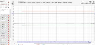
Here's my dual 1541 DAC. Input is spdif direct from a Behringer UAC222 into a SRC24/96 set to upsample to 96Khz, and output from the Sowter transformer into the 22k input Z of the UAC.
Show me where the frequency reponse is influenced by the inductance, and relatively low load impedance.
Green line is phase.
Rather than all the theory and opinions, I like to present actual results.....
Show me where the frequency reponse is influenced by the inductance, and relatively low load impedance.
Green line is phase.
Rather than all the theory and opinions, I like to present actual results.....
Attachments
Interesting. That would suggest that the harmonics profile posted at MVlabs corresponds to listening experiences (I do not agree here with Thorsten that the level matters more than the harmonic profile). I also remember reading reports from early 2000's where ppl preferred higher R.John has changed his mind on the IV resistor value. He was in favour of very low values because it wa claimed to produce least distortion.
Then he decided that a higher value (~75 I think) sounded better.
I didn't like the sound when I tried a much lower value - it compressed the audio and gave it a lifeless sound.
Apologies Icsazar no punt intended, appreciate your experiment & sharing with us of your findings. The reason that I brought up your thread here is sincePlease note that the voltages on the conceptual schematics of the TDA1541A in the opening post are written in reverse order. Also you can't measure the voltages directly because the input resistance (usually 10M) of the measuring instrument falsifies the actual value. I used the compensated bridge method.
we're able to null the differences on the DEM pins, would that negate the need of using big capacitors or if we can take your ideas & expound on it further.
Cheers
Thanks Thorsten for sharing.
I understood it all, with the exception of the JFET compounds. Could you explain them in detail? I don't get how they work.
(BTW I understand the BJT compound).
It is deliberately drawn a little misleading. It is the same as a simple Darlington, but with a J-Fet. As the J-Fet has a limited drain source voltage, it is powered by a zener diode. How this diode gets it's current without allowing "current escape" or adding extra current AND being able to have the circuit start is the magic trick, I wish to keep hidden. Sorry.
But functionally it's just a Darlington with an N-J-FET instead of first NPN in redux.
Did You tried ES9008, first model?
I never even had the EVM.
I just found it 🤢
it is min -0.3V and max +0.3V
Where did you find that? Curious.
Thor
Hi Thorsten if I may, what are your thoughts on this thread https://www.diyaudio.com/community/threads/tda1541a-reducing-dnl.414159/
Interesting.
Seeing TDA1541 well implemented is -95dB THD&N and -110dB SNR at digital silence, which is adequate for 18 bit @ 96kHz (dithered at 384kHz - not that anyone made CPLD code for it, though trivial), I will question the purpose though.
Thor
I do not agree here with Thorsten that the level matters more than the harmonic profile.
I do not agree with this guy either. Wait, that's supposed to be me? No, I was not talking about level.
Thor
In the datasheet?Where did you find that? Curious.
But Vgnd(d) signed with "-" is that telling us that only negative PS are digital part
And Vgnd(d) is refering to +5V?
So that is obviously if the power suplies are separate. BUT which one or ALL of them.
+5V is digital for sure?
-5V ?
-15V ?
So if we can be for sure what the suplies are D and A, we can left open connection with AGND and DGND and measure eventual difference?
I dont know if it is from the importance but GND(D) is close to Vdd2 -15V (to decouple)
That can implicate that -15V is digital PS?
Also GND(A) is closer to AOR and AOL, somehow logical. But next close to Vdd1 -15V and Vdd +5V
.
The pins are far away from each other, diagonal, are Vdd and GND(D) which has to be closest to decouple?
Last edited:
You still need appropriate filter capacitors (decoupling in Philips' terms) according to your taste, beliefs and superstitions.Apologies Icsazar no punt intended, appreciate your experiment & sharing with us of your findings. The reason that I brought up your thread here is since
we're able to null the differences on the DEM pins, would that negate the need of using big capacitors or if we can take your ideas & expound on it further.
Cheers
It is deliberately drawn a little misleading. It is the same as a simple Darlington, but with a J-Fet. As the J-Fet has a limited drain source voltage, it is powered by a zener diode. How this diode gets it's current without allowing "current escape" or adding extra current AND being able to have the circuit start is the magic trick, I wish to keep hidden. Sorry.
I could use one A23 alkaline battery to achieve low current escape, circuit below. Single digit nanoamp base current modulation on Q2. The circuit is biased by I1 which is 10mA, the signal is I2 which is 2mA P-P. The squarewave looks good with 300nF+200mohm.
HOWEVER, the simulated distortion is high, second harmonic is 60dB down from the fundamental (10 KHz). This shouldn't be, it doesn't make sense. What's happening here?
Last edited:
In the datasheet?
Too many floating around, it's not in the ones I have.
But Vgnd(d) signed with "-"
No, it is not.
It is:
Vagnd - Vdgnd = -0.3V ... + 0.3V.
is that telling us that only negative PS are digital part
No. It's just a line break.
And Vgnd(d) is refering to +5V?
No, it is referring to DGND.
I will agree, based on that.
BUT which one or ALL of them.
Based on internal Circuit details published, AGND/-15V are one pair, DGND/+5V are another pair and -15V is kinda at loose ends but really loops to +5V.
+5V is digital for sure?
No, it is MOSTLY digital but also carries the complement of Iout.
-5V ?
My best guess, DC and digital CCS common.
-15V ?
= True Analog Reference Pin
So if we can be for sure what the suplies are D and A, we can left open connection with AGND and DGND and measure eventual difference?
We can, but the risk is a dead chip.
We know no power pin draws > 50mA, so if we connect a resistor of 0.3V/50mA = 6 Ohm between the grounds (say 3R3 to be safe) we can measure current.
I dont know if it is from the importance but GND(D) is close to Vdd2 -15V (to decouple)
No, Vdd (+5V) and Vss (DGND) are placed in line with standard practice for (TTL/ECL) the logic IC of the era (still observable in modern 74HCXX CMOS logic).
That can implicate that -15V is digital PS?
No.
Also GND(A) is closer to AOR and AOL, somehow logical.
Not really.
The pins are far away from each other, diagonal, are Vdd and GND(D) which has to be closest to decouple?
All TTL pinout derived IC's are like that.
Compare 74HC74 to 74ACT11074.
Thor
- Home
- Source & Line
- Digital Line Level
- Building the ultimate NOS DAC using TDA1541A