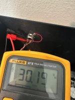
It looks like it's not. PSU ground pin is 30V above chassis ground...@jf4828
Maybe I can't see it well, but where is the ground from your PS board connected? How is it connected to chassis ground?
Best,
Anand.

So sounds like I've failed to connect PSU ground to chassis...... Chassis ground and psu ground measure as an open circuit....
Dang, you're quick.
Measure to the lug on the chassis floor. I added a snippet above likely after you read it to do a quick resistance check between all pins within and between the jacks.
What's the black probe connected to? Why? ..... if the red wire "works"... then that connects pin 1 to the chassis. There should be 0V between pin 1 and the chassis pretty much by definition.
Best place for takeoff is the back junction jumper of the PSU that you have soldered. But before you do that, I would measure resistance between PSU gnd (mentioned jumper) and chassis, heck, even a voltage DC and AC measurement can’t hurt. Can’t hurt to also measure resistance between MOSFET middle pins and chassis too (amp off), but it looks like you have mounted the fets before soldering them so that test I expect to end up in Mohms or the high K’s.So sounds like I've failed to connect PSU ground to chassis...... Chassis ground and psu ground measure as an open circuit....
The black probe is essentially connected to chassis. There are 4 connection points on the XLR socket. Pins 1,2,3 + chassis. Let me try the measurements you mentioned...
........ or - open circuit (Ol), if you didn't connect these two in any wayfirst check continuity between audio GND (GND on cap bank) and case; of course while amp powered off
it's either 0R if you did directly connect GND and case/safety GND, or 10-ish ohms, if there is NTC between audio GND and case/safety GND
which you must
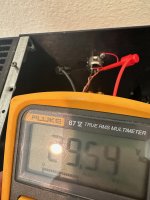
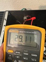
VAC between PSU and chassis is indeed 30. DC voltage is effectively 0. Resistance between middle pin of MOSFET and chassis is open.Best place for takeoff is the back junction jumper of the PSU that you have soldered. But before you do that, I would measure voltage DC and AC between PSU gnd (mentioned jumper) and chassis. Can’t hurt to measure resistance between MOSFET middle pins and chassis too, but it looks like you have mounted the fets before soldering them so that test I expect to end up in Mohms or the high K’s.
Disconnect the amplifier boards from the power supply, then check the DC voltage at the power supply. Start with voltage at the + and - terminals of the bridge rectifiers. DC or AC from the bridge rectifiers?
Maybe... maybe not...The black probe is essentially connected to chassis. There are 4 connection points on the XLR socket. Pins 1,2,3 + chassis. Let me try the measurements you mentioned...
IF it were connected to the chassis... and IF pin 1 was connected to the chassis, then there would be 0V between pin 1 and the chassis.
Anyway... you've got too many people typing to you all at once. I'll bow out.
But... that's why I advised taking the measurements to the mains earth / safety ground lug on the chassis floor also... if mains earth is to be your ground reference... start there.
Last edited:
Thanks all... Ran back through build documentation and indeed I missed that ground connection 😢. I've connected PSU ground and everything seems to be functioning and measuring correctly now.......
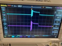
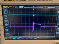
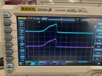
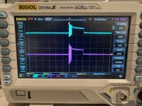
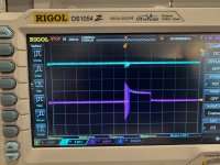
So decided to do some more testing so want to verify what I'm seeing looks correct before hooking up another $2k interface🙂 The teal colored trace is measurement between XLR pins as labeled in picture file name. The purple trace is measurement at speaker terminals.... Most of these are capturing power off. The Single on a smaller time scale is power on... I'm guessing that since what I'm connecting to produces +24dBU signals I should be safe with this.... I'm not too worried about the speaker thump and realize the measurements unloaded aren't completely valid...
Attachments
Last edited:
Hi everyone - I need to come here for confession, shaming, and encouragement. I started my build around 2 years ago, got as far as having the power supply finished/tested, and a new job, cross country move, etc. distracted me. I just saw the announcement of the new Jzm, and that finally gave me the encouragement to get this project across the finish line.
Hello,
I know this has been addressed before, but I had an idea for inverting the Jfet input stage in order to allow the use of LSK170 or LSK389 (in my case I plan to use LSK489). I've seen versions where the N channel Jfets were the opposite of the orientation I propose, but I'm not used to seeing negative voltage applied to the drain and positive to the source. I just want to know if this makes sense &/or if there are things I could change. Also I inverted Q2 (CCS).
Thanks for your time.
Well, Q2 isn’t going to work as a current source like that.
I believe the N-channel Jfets will not bias correctly even if Q2 is corrected.
I believe the N-channel Jfets will not bias correctly even if Q2 is corrected.
Hmm, so even with Q2 as the normal PNP, that wouldn't bias right. Given Vgs being positive(?) here. I suppose it makes sense then why the source and drains are reversed in other designs.
Thanks for your time
reasons why that isn't going to work are on too low/basic level to be clever/useful to explain in one or few posts in thread
I mean, question shows that you're lacking basic knowledge of basic parts operation; when you learn basics, you'll have explanation to today's question ..... and then you'll be able to think further;
There are numerous sources ( books, on-line) so learning is easy
We all were in same boat - really wishing to write a love poem, even before learned entire alphabet
- Home
- Amplifiers
- Pass Labs
- Aleph J illustrated build guide