R32 (0.22 ohm) is currently connected to the output connector of this board.What about the output inductor and output series resistor? Are these to be mounted off-board?
I presume you mean the resistor that goes in parallel with the output inductor. On all the other boards I've seen on this thread, the output inductor and parallel resistor are mounted off-board.
I'll have a look at the size of the inductor/resistor and see about mounting them onboard. Ideally without extending the pcb length any further.
Geoffw1,
What is the diameter of the mosfet fastener holes? They look a bit small for the fastener head to fit through.
What is the diameter of the mosfet fastener holes? They look a bit small for the fastener head to fit through.
The holes for the fasteners are those set in the KiCad 8 footprints for both the single die and double die versions of the MOSFETs as horizontal up profiles. I'll check in the morning and adjust as necessary.What is the diameter of the mosfet fastener holes? They look a bit small for the fastener head to fi8through.

I've reviewed a few things related to the last few responses.
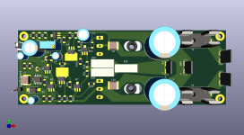
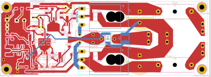
- The output inductor/resistor (Thiele network) take up too much room to sensibly integrate into a 50mm width pcb (this width done to accommodate the Modushop Dissipante heatsink bracket dimensions) so I'm sticking with these being mounted off-board between this pcb and the output terminals mounted on the case.
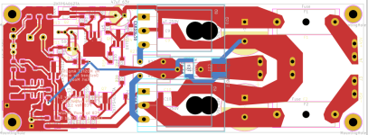
- The KiCad8 footprints for the MOSFETS (both single and double die options) have a 3.3mm diameter for the fastener holes. These are fine if mounting directly to the PCBs but need to be larger (7mm dia) when mounting MOSFETS onto the heatsink which is spaced off from the pcb by around 10mm or so (can't remember what Mooly originally stated). The larger holes are now incorporated in the board layout and tracking around their locations adjusted accordingly.
Attachments

It looks like your component numbering isn't following the original schematic? For example, I see R31 as a SMD resistor on the bottom layer. This doesn't correspond to the schematic from Post #1.
I'd suggest updating the numbering to match the Mooly's Post 1 schematic.
I'd suggest updating the numbering to match the Mooly's Post 1 schematic.
Looks good work to these uneducated eyes.I've reviewed a few things related to the last few responses.
Unless someone comes up with anything else important, this will be the final layout and here's the gerber
- The output inductor/resistor (Thiele network) take up too much room to sensibly integrate into a 50mm width pcb (this width done to accommodate the Modushop Dissipante heatsink bracket dimensions) so I'm sticking with these being mounted off-board between this pcb and the output terminals mounted on the case.
- The KiCad8 footprints for the MOSFETS (both single and double die options) have a 3.3mm diameter for the fastener holes. These are fine if mounting directly to the PCBs but need to be larger (7mm dia) when mounting MOSFETS onto the heatsink which is spaced off from the pcb by around 10mm or so (can't remember what Mooly originally stated). The larger holes are now incorporated in the board layout and tracking around their locations adjusted accordingly.
Could a seperate pcb be made for the inductor, resistor?
Agreed it's worth keeping consistency across the whole thread as far as the schematic numbering is concerned. I'll get back on it and repost pics, schematic and gerber shortly.I'd suggest updating the numbering to match the Mooly's Post 1 schematic.
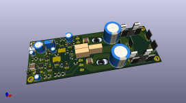
Schematic component numbering revised to match originals so we now have consistency with Mooly's original. Here we go!
Attachments
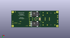


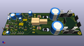
I notice the MOSFETs are facing the wrong way in the 3D rendering. It appears to be just the 3D model and the footprint itself is OK.
I had problems finding a decent 3d model for the package type in the relevant horizontal orientation. As you say, the footprints are correct for both packets types.
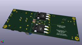
May be my comment is late: by mounting the mosfets on the same vertical line, is not the efficiency of heat sink utilization compromised ?
Reasonable question.
If the amplifier were to be run continuously at high power levels, it could be an issue but for domestic use isn't a problem.
The quiescent state with output bias set to give 100mA through the MOSFETs will dissipate about 4W in each MOSFET. and won't be much more at domestic (even a noisy party) levels.
A few posts back I uploaded the schematic and renderings for the revised layout with component numbering matching Mooly's original. I forgot to upload the Gerbers to go with it. Here they are if anyone cares to use them. I've just ordered a min quantity of 5 from JLCPCB so, once I extract 2 for myself, will have a couple spare and am happy to pass them on for cost of postage (within UK) if anyone is interested.Schematic component numbering revised to match originals so we now have consistency with Mooly's original. Here we go!
Attachments
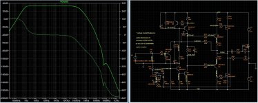
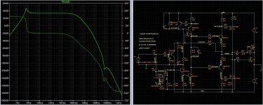
There’s an extensive discussion about this a few pages back. Essentially, increasing the cap to resolve this hump increases the servos settling time.
All gone! 🙂I've just ordered a min quantity of 5 from JLCPCB so, once I extract 2 for myself, will have a couple spare and am happy to pass them on for cost of postage (within UK) if anyone is interested.
Nice to see this thread active since it started in March 2008.
Thanks for sharing your SMT layout and BOM of Mooly’s amp Geoffw1 😉.
I’ll be placing an order shortly and will have a few extra, if in the USA pm me if interested.
I’ll be placing an order shortly and will have a few extra, if in the USA pm me if interested.
- Home
- Amplifiers
- Solid State
- My MOSFET amplifier designed for music