yes, that was the textbook in that class 40 years ago.https://www.worldradiohistory.com/B...nce-Curve-Design-Manual-Pullen-1958-Adobe.pdf
This is a calculation of the screen resistor.
Minimum noise will be with 0R grid resistor, however this can result in VHF oscillation and/or rectification of radio stations. The equivalent grid noise resistance for a triode is approximately 2.5/gm so using a grid resistor of somewhat less than this will be the thing to do. There's also plate noise too to consider. 1meg is noisy as that's what guitar inputs use before you plug the pickup in.
Show me how to make one of those beam triode regulator tubes like the 6HV5A unconditionally stable without resistors, chokes and RF bypass caps with near zero lead length on nearly every pin - Easy don't apply any heater voltage and keep it in its box.
the guitar amps usually have a 47-68K coupling resistor and maybe a 1M bias stabilizing resistor, but its not a grid stop. Even though the DC coupling resistor would act as one.There's also plate noise too to consider. 1meg is noisy as that's what guitar inputs use before you plug the pickup in.
What can I learn from you about those wide (what I assume are ground) traces?and laid out a PC board for it.
Attachments
I tried to keep the question brief as i wasn't even sure how to ask. Your experience is too great to have made those traces at random. I was asking you to learn what the thought was. I don't know enough about RF to make any assumptions other than think , well he was doing that kind of stuff at Motorola so maybe . . . . but if it's some sort of shielding , I would have guessed you'd want a plane covering the whole board. Or is it heat sinking?
Thanks
Thanks
I learned how to design PC boards the hard way, by screwing up a few zillion before getting them right. In the early years I made some PC boards for transistorized stuff that I had created, but most were simple things like guitar pedals or preamps that fed a known power amp, usually a clone of one of the SWTPC Tiger series amps. Most actually worked but could have worked better. By the early 70's I built very little tube stuff, and it was all guitar amps or ham radio RF amps.
In 1975 I bought one of the SWTPC MC 6800 computer kits that used the SS-50 bus. A few of my coworkers at Motorola and I cloned it using DIY boards that were photographically copied from the originals. Then I designed my first memory expansion board for the SS-50 bus. It kinda worked, but mostly didn't. Random memory errors came and went whenever they wanted to. We worked at the company that invented the MC 6800 chip, so we sought out some experts. They laughed at my PC board attempt, explained a few things like "ground bounce" and the need for wide traces for ground. It seems that narrow traces have sufficient inductance to develop a voltage pulse on the end of a long ground trace if a few CMOS gates change states at the same time. A true CMOS chip operated well within its speed rating draws nearly zero current in operation. Current is only drawn during a state change when the N and P fets are partially on at the same time. We had 8 and 16 memory chips all on the same ground trace. My second board was much less dense, had fat traces and worked quite well. we went on to make more memory boards, a color graphics board, and even a 68HC11 processor board for the SS-50 bus.
There were no microprocessor people in our plant early on all the engineering done in our plane was done at RF. The principles are the same, only the RF stuff can be worse as the frequencies go up. The old SWTPC computer ran at a blazing 921 KHz! The walkie talkies we made when I started in 1973 worked up to 512 MHz and by the time I got into engineering they ran at up to 931 MHz.
There is another reason for fat traces, and it only applies if you make your own PC boards. A DIY pc board starts with a layer of copper on both sides. It is covered with something that keeps the copper from being etched away during the etching process. In my case it is Laser Printer toner. The uncovered copper gets etched away with an acidic solution while the covered areas remain. The toner is them removed with acetone leaving the desired pattern on the fiberglass board. The more copper you have to remove, means more chemicals get used up, so I try to leave large copper areas whenever possible.
The wide traces for ground generally will not hurt anything with a few exceptions, and can help lower any inductance in a ground path. Many PCB designers use a copper pour technique that will fill all empty space on a PC board with ground, given a pre-defined distance between ground and anything else. This technique has merits for most board designs and I have attempted to do it manually in the 15 year old version of Eagle that I use for most of my boards. Most of the boards I did at Motorola did use solid copper "pour" everywhere on each layer that didn't have an active trace. This will generally create the lowest noise board with the lowest radiated unwanted spurious emissions.
Vacuum tube amps often operate at high impedances and often high voltages. In these cases one must be mindful of the spacing between a voltage carrying trace and ground. One also might not want a ground fill on the opposite side of a very high impedance trace as the extra capacitance created between that trace and ground on the other side may create an unintended rolloff of the higher frequencies. This is usually not a problem in a vacuum tube audio amp, but may become an issue at RF.
Things get much more complicated in a cell phone or multi-band walkie talkie board that encompasses digital, analog audio and RF technology on the same small PC board. The board is usually multiple layers often using more than one technique between the individual layers. There is at least one layer that is all ground plane. The last walkie talkie test board that I laid out at Motorola had 10 copper layers. Four layers used three slices of 10 mil thick conventional PCB material in the middle with three HDI layers on each side on top of that. An High Density Interconnect layer is essentially an insulating layer of thick solder mask between copper layers. There are conventionally drilled holes for the instances where a hole goes completely through the board. Holes on the HDI layers on either side of the sandwich are laser drilled. Here SMD parts are placed on both sides of the board. Usually there is at least one layer that is all ground. This board had two ground layers and one that was mostly ground except for power distribution.
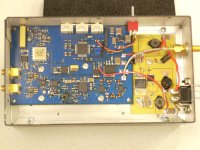
The picture shows a medium power (10 watt peaks) LTE transmitter that I designed and built 5 of. They operated from 150 to 950 MHz and were used to demonstrate a new technology to the FCC for possible approval. These units were programmed for use from 470 MHz to 695 MHz only and the parts values were adjusted for maximum performance over this range. The blue board does all the RF and digital stuff. It has four conventional layers. The green board is the power supply it has only two layers. The same copper pour technique was used on both to minimize spurious RF emissions since they were going to be tested by the FCC. Note the zillions of tiny holes that connect the grounds on all the layers together. This is important in RF boards.
In 1975 I bought one of the SWTPC MC 6800 computer kits that used the SS-50 bus. A few of my coworkers at Motorola and I cloned it using DIY boards that were photographically copied from the originals. Then I designed my first memory expansion board for the SS-50 bus. It kinda worked, but mostly didn't. Random memory errors came and went whenever they wanted to. We worked at the company that invented the MC 6800 chip, so we sought out some experts. They laughed at my PC board attempt, explained a few things like "ground bounce" and the need for wide traces for ground. It seems that narrow traces have sufficient inductance to develop a voltage pulse on the end of a long ground trace if a few CMOS gates change states at the same time. A true CMOS chip operated well within its speed rating draws nearly zero current in operation. Current is only drawn during a state change when the N and P fets are partially on at the same time. We had 8 and 16 memory chips all on the same ground trace. My second board was much less dense, had fat traces and worked quite well. we went on to make more memory boards, a color graphics board, and even a 68HC11 processor board for the SS-50 bus.
There were no microprocessor people in our plant early on all the engineering done in our plane was done at RF. The principles are the same, only the RF stuff can be worse as the frequencies go up. The old SWTPC computer ran at a blazing 921 KHz! The walkie talkies we made when I started in 1973 worked up to 512 MHz and by the time I got into engineering they ran at up to 931 MHz.
There is another reason for fat traces, and it only applies if you make your own PC boards. A DIY pc board starts with a layer of copper on both sides. It is covered with something that keeps the copper from being etched away during the etching process. In my case it is Laser Printer toner. The uncovered copper gets etched away with an acidic solution while the covered areas remain. The toner is them removed with acetone leaving the desired pattern on the fiberglass board. The more copper you have to remove, means more chemicals get used up, so I try to leave large copper areas whenever possible.
The wide traces for ground generally will not hurt anything with a few exceptions, and can help lower any inductance in a ground path. Many PCB designers use a copper pour technique that will fill all empty space on a PC board with ground, given a pre-defined distance between ground and anything else. This technique has merits for most board designs and I have attempted to do it manually in the 15 year old version of Eagle that I use for most of my boards. Most of the boards I did at Motorola did use solid copper "pour" everywhere on each layer that didn't have an active trace. This will generally create the lowest noise board with the lowest radiated unwanted spurious emissions.
Vacuum tube amps often operate at high impedances and often high voltages. In these cases one must be mindful of the spacing between a voltage carrying trace and ground. One also might not want a ground fill on the opposite side of a very high impedance trace as the extra capacitance created between that trace and ground on the other side may create an unintended rolloff of the higher frequencies. This is usually not a problem in a vacuum tube audio amp, but may become an issue at RF.
Things get much more complicated in a cell phone or multi-band walkie talkie board that encompasses digital, analog audio and RF technology on the same small PC board. The board is usually multiple layers often using more than one technique between the individual layers. There is at least one layer that is all ground plane. The last walkie talkie test board that I laid out at Motorola had 10 copper layers. Four layers used three slices of 10 mil thick conventional PCB material in the middle with three HDI layers on each side on top of that. An High Density Interconnect layer is essentially an insulating layer of thick solder mask between copper layers. There are conventionally drilled holes for the instances where a hole goes completely through the board. Holes on the HDI layers on either side of the sandwich are laser drilled. Here SMD parts are placed on both sides of the board. Usually there is at least one layer that is all ground. This board had two ground layers and one that was mostly ground except for power distribution.
The picture shows a medium power (10 watt peaks) LTE transmitter that I designed and built 5 of. They operated from 150 to 950 MHz and were used to demonstrate a new technology to the FCC for possible approval. These units were programmed for use from 470 MHz to 695 MHz only and the parts values were adjusted for maximum performance over this range. The blue board does all the RF and digital stuff. It has four conventional layers. The green board is the power supply it has only two layers. The same copper pour technique was used on both to minimize spurious RF emissions since they were going to be tested by the FCC. Note the zillions of tiny holes that connect the grounds on all the layers together. This is important in RF boards.
Attachments


Thanks ! As I expected you're the Santa Claus of valuable experience, if that makes any sense.
(It's the time of year so forgive me coming up with that one.)
Those zillions of holes , is that so that all planes will carry the same currents ?
To equalize the potential between ”grounded” planes. At the RF frequency where a wave actually travels along it. Omit too many of those vias and the RF lines between the planes don’t behave as 50 or whatever ohm lines anymore. You can even get multiple modes instead of a single TEM mode and everything you assume about the circuit breaks down. Yeah, you can simulate it with the proper tool. Often you won’t like the result. And lacking the proper 3D simulation tool you just have to make the assumption about how close the vias need to be in order for your 2 or 2.5D result (or just an impedance calculator, if that’s all you’ve got) to be valid.
This is the first time I've heard of Transverse Modes so reading to do but in the meantime would it be correct to think of the vias as eliminating localized capacitances between planes ?
The idea for all of the holes is to force all of the ground planes to function as one thick ground plane. This is real important in applications like a walkie talkie where the radio's chassis, board and housing act as the counterpoise for the end fed antenna. Basically, the visible whip antenna is half of a dipole while all the metal elements in the radio are the other half. The user's hand is also part of the antenna system, albeit a rather lossy part. You want as much of that "external" RF current kept as far away from sensitive circuits as possible.
Most of the boards I did at Mot operated between 100 MHz and 1 GHz. I usually used a 0.05 inch routing grid for low density boards like the test boards seen in the picture. The hole spacing was usually set to a multiple of that and often varied across the surface of the board. It looks like I used a 0.1 hole grid and a 2 X or 5 X fill (every second or fifth grid point gets a hole) pattern for the blue board.
For vacuum tube boards, I usually just stick holes where it looks like they are needed. I dug the old Spud board out of the "box of dead circuits" and looked it over. It looks like something I did on the spur of the moment in a big hurry, so I looked back into my Eagle and PICTURES folders. There is a July 4, 2008 date on the board itself.
The pictures of the furball of clip leads on an SSE board all have the same June 21 2006 date on them. This wrong since the old Sony camera lost its date data every time the battery ran down, but all have the same June date. Most of the pictures showing the PC board are dated July 6, 2008.
There are two "SPUD" folders in the Eagle Projects directory, both from July 4, 2008. It looks like the schematic was done between 4:27 PM and 6:14 PM. The board took from 5:08 PM until 10:43 PM. It would appear that I made the PC board itself and populated it between the 5th and 6th of July, so yes this was a rush job. The quality of the board itself shows that. Every trace has bad spots, but the board still works after I fixed a broken trace resulting from over 10 years in the "box." The yellow LED on the right had been pushed into the board breaking the trace on the bottom. A little solder fixed it.
Attachments
OK I see . (about the holes)
What about other traces besides the wide grounds? I did see your comment on saving chemical but I'm also curious about your factory boards and how you size them. I have a friend who used to do tube amp boards with traces so narrow I wanted to say " Hey man, they're not charging for copper, live a little, leave some on." (I actually did say it once but it was clear he wasn't in a debating mood.) I think he used a calculator and sized everything for technical minimum . A one millimeter trace would leave a half inch of bare space between it and the next one over. About the only advantage I could see was that the pads were easy to heat.For vacuum tube boards, I usually just stick holes where it looks like they are needed
This is also true of cell phones isn't it?The user's hand is also part of the antenna system, albeit a rather lossy part.
I am still using an old version of Eagle for my vacuum tube PC board layouts. When Cadsoft was bought out by Newark / Farnell many years ago they wanted nearly $800 for a new "PRO" version of Eagle that could handle the board size used in tube amps even though they were really simple compared to a processor board or any of the digital stuff that was trendy at the time. Things got even worse when Autodesk bought Eagle and now wants $600 per year for a license. My old version does not do copper pour or fill so all ground fills are made with overlapping 0.100 inch traces.
When I start down the road to a vacuum tube board I set the trace width to 0.050 inch. This is thick enough that an inexperienced builder is not likely to lift or otherwise destroy a trace while trying to solder or desolder something. That is my default width for everything. I rarely go smaller on a tube amp board, but I will use thicker traces where needed like for heater power.
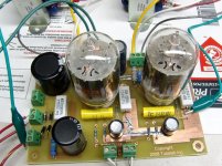
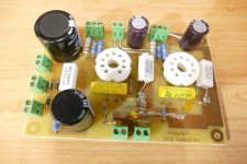
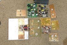
I will almost always manually fill the outer edges with copper ground plane, and fill wherever I think a good solid ground is needed or wanted. I will usually do a test board at this stage to find out if the idea works and is worth taking any farther. The board in the first picture is a high gain guitar preamp with 4 stages of 12AX7 which will pickup hum and noise like a magnet. I threw down lots of ground on both sides from the get-go. It worked on the first try, but it was a copy of a known good schematic.
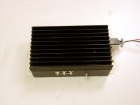
The next picture shows a few boards. The four in the lower right side are all versions of my Universal Driver boards. I was never happy with any of them. The final board is larger and came a couple years later than these. The board in the lower center is the prototype of the TSE-II it worked as intended on the first try, so I got some boards made at a board house and stripped this one for most of its parts. You can see the extensive grounding on the other side of the board along the right side. This is the input area where susceptibility to hum is the greatest, so I filled most of the area with ground. The board on the copper heat spreader in the heat sink is a 500 watt RF power amp for ham radio use in the 1.8 to 50 MHz range. It is mostly ground as are most RF boards. A bare unpopulated board is above it on the carpet. The green board is the commercial version of the original TSE amp. The DIY proto board is to it's right. It was the first Tubelab board. It was in my Lexan TSE for several years until I replaced it with a shiny green board.
Most of my ground fill areas are my attempts at emulating what the super expensive Mentor Graphics software did at work. A team of experts spent a couple years of tweaking the setup on the Mentor stuff to do a good job on all the different boards we did at Mot. I made a lot of test boards and prototypes at Motorola. I had drop down menus on my workstation to choose a 2 layer, or 4 layer board. There were several other more complex choices, but I rarely used them. After placing all the parts and routing the board, I let the software fill in the ground everywhere according to design rules chosen by the board experts. That's how the blue and green boards in the previous post were done.
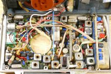
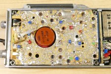
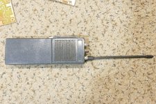
The picture of a Motorola HT-220 walkie talkie is an example of the first radio I saw when I walked into Motorola in 1972. It was designed in the late 60's and produced until the late 70's. This particular unit was made in late 1976 so it was one of the last ones made. The board was laid out with tape on Mylar and reproduced photographically. I did my SS-50 computer memory boards the same way in the 70's.
The whip antenna on the top is half of a dipole with the metal frame functioning as the other half. This is the ideal case for a portable radio device. Note the way the board is routed with ground everywhere it could possibly go, and metal strapping added to reinforce the ground plane in sensitive areas. I learned to respect ground right here!
I spent a year and a half in the factory fixing, tuning, finally assembling, and testing them before shipment to the customer. In these days all of the boards were hand stuffed with through hole parts, tiny ones at that. There are over 400 parts on this board. Virtually every radio built in the early 70's had something wrong with it. All had to be touched by experienced technicians before several rounds of manual testing occurred. I was one of them. After all of this, they were baked in an oven, frozen and tested again.
The antenna inside a cell phone is a bit different. A phone must operate over a wide range of frequencies from about 600 MHz up to 2.5 GHz. The antenna is a compromise made to cover a wide bandwidth and fit in a tiny spot inside the phone. Often there are two or more antennas made on the PC board itself, or on a high dielectric ceramic substrate placed somewhere inside the phone. The user's hand will absorb a good deal of the RF energy in the higher frequencies so often the antenna is aimed to shoot through the screen at a low angle in hopes of getting past as much human tissue as possible. Sometime there is a second antenna along the top edge. Every phone is different, and I have not looked inside any phone made in the last 10 years, so things have likely changed a bit since I took one apart. When we actually made phones in Florida we took them to an antenna lab at a local university for testing. I happened to get my master's degree at that school so I got to play in that lab a bit. When we first started putting GPS technology inside the phone our prototype antennas were late and we needed to test the radio hardware. I sat down at a RF network analyzer and created a 1.5 GHz "J" antenna out of a paper clip and tested it in that lab. It worked as good as the real antennas did once they finally arrived.
When I start down the road to a vacuum tube board I set the trace width to 0.050 inch. This is thick enough that an inexperienced builder is not likely to lift or otherwise destroy a trace while trying to solder or desolder something. That is my default width for everything. I rarely go smaller on a tube amp board, but I will use thicker traces where needed like for heater power.
I will almost always manually fill the outer edges with copper ground plane, and fill wherever I think a good solid ground is needed or wanted. I will usually do a test board at this stage to find out if the idea works and is worth taking any farther. The board in the first picture is a high gain guitar preamp with 4 stages of 12AX7 which will pickup hum and noise like a magnet. I threw down lots of ground on both sides from the get-go. It worked on the first try, but it was a copy of a known good schematic.
The next picture shows a few boards. The four in the lower right side are all versions of my Universal Driver boards. I was never happy with any of them. The final board is larger and came a couple years later than these. The board in the lower center is the prototype of the TSE-II it worked as intended on the first try, so I got some boards made at a board house and stripped this one for most of its parts. You can see the extensive grounding on the other side of the board along the right side. This is the input area where susceptibility to hum is the greatest, so I filled most of the area with ground. The board on the copper heat spreader in the heat sink is a 500 watt RF power amp for ham radio use in the 1.8 to 50 MHz range. It is mostly ground as are most RF boards. A bare unpopulated board is above it on the carpet. The green board is the commercial version of the original TSE amp. The DIY proto board is to it's right. It was the first Tubelab board. It was in my Lexan TSE for several years until I replaced it with a shiny green board.
Most of my ground fill areas are my attempts at emulating what the super expensive Mentor Graphics software did at work. A team of experts spent a couple years of tweaking the setup on the Mentor stuff to do a good job on all the different boards we did at Mot. I made a lot of test boards and prototypes at Motorola. I had drop down menus on my workstation to choose a 2 layer, or 4 layer board. There were several other more complex choices, but I rarely used them. After placing all the parts and routing the board, I let the software fill in the ground everywhere according to design rules chosen by the board experts. That's how the blue and green boards in the previous post were done.
The picture of a Motorola HT-220 walkie talkie is an example of the first radio I saw when I walked into Motorola in 1972. It was designed in the late 60's and produced until the late 70's. This particular unit was made in late 1976 so it was one of the last ones made. The board was laid out with tape on Mylar and reproduced photographically. I did my SS-50 computer memory boards the same way in the 70's.
The whip antenna on the top is half of a dipole with the metal frame functioning as the other half. This is the ideal case for a portable radio device. Note the way the board is routed with ground everywhere it could possibly go, and metal strapping added to reinforce the ground plane in sensitive areas. I learned to respect ground right here!
I spent a year and a half in the factory fixing, tuning, finally assembling, and testing them before shipment to the customer. In these days all of the boards were hand stuffed with through hole parts, tiny ones at that. There are over 400 parts on this board. Virtually every radio built in the early 70's had something wrong with it. All had to be touched by experienced technicians before several rounds of manual testing occurred. I was one of them. After all of this, they were baked in an oven, frozen and tested again.
The antenna inside a cell phone is a bit different. A phone must operate over a wide range of frequencies from about 600 MHz up to 2.5 GHz. The antenna is a compromise made to cover a wide bandwidth and fit in a tiny spot inside the phone. Often there are two or more antennas made on the PC board itself, or on a high dielectric ceramic substrate placed somewhere inside the phone. The user's hand will absorb a good deal of the RF energy in the higher frequencies so often the antenna is aimed to shoot through the screen at a low angle in hopes of getting past as much human tissue as possible. Sometime there is a second antenna along the top edge. Every phone is different, and I have not looked inside any phone made in the last 10 years, so things have likely changed a bit since I took one apart. When we actually made phones in Florida we took them to an antenna lab at a local university for testing. I happened to get my master's degree at that school so I got to play in that lab a bit. When we first started putting GPS technology inside the phone our prototype antennas were late and we needed to test the radio hardware. I sat down at a RF network analyzer and created a 1.5 GHz "J" antenna out of a paper clip and tested it in that lab. It worked as good as the real antennas did once they finally arrived.
Attachments
Last edited:
People with lots of experience often talk about the circuit on the board but it's less often they talk about their thinking / approach to putting it together, so your posts are pretty valuable to me, but there's a lot of information in what you write so it takes a few readings and a couple of days pondering to sift through and figure what questions are still there.
" I will almost always manually fill the outer edges with copper ground plane, . . . ." , So does that end up being used like a buss or do you tie it into the circuit in a way that prevents current flow around it? Is it even something that needs thinking about?
Re: "This is the input area where susceptibility to hum is the greatest, so I filled most of the area with ground." I could ask this two different ways for a tube audio circuit :
1) If the copper is already there on the board material , why not just leave ground plane everywhere something else isn't? (Like in the board on the upper right in pic 4)
or
2) Are there places/situations where it's better not to have ground plane of any size around? (Besides the capacitance to high impedance trace on RF board situation which you already mentioned above)
One only half related question . Does mounting an audio transformer directly on a ground plane help to make the general circuit quieter by virtue of shielding or noisier by inducing local currents in the ground plane? I've got a not quite fur-ball level breadboarded two stage amp with interstage transformer that I"m trying to get very low noise output from and wondering whether rebuilding the whole thing on a piece of copper clad will be worth the trouble. Any advice on that?
About the cellphone antenna, I once (maybe six or seven years ago) got into a coffee shop back and forth with a fellow at the next table who turned out to be an engineering prof at the local university. The prof and his crew were working on something to do with RF communications and cell phones and when I asked him if wired earphones acted as antennas he lit right up with a big "Oh Yes ! We took a good look at that and . . . . ." I don't remember all the details of his explanation now, only that I walked away from that conversation thinking it was probably best not to take them for granted and use them too much.
As always, Thank you!
The concept of making a border around the outside edge of the PC board comes from the process I use in the making of a DIY PC board. Having aa nice rectangular pattern on both sides of the board make it easier to line the two sides up with each other.
I got a bunch of large (about 200 by 400 mm) double side copper clad board stock at a hamfest close to 40 years ago. I find it easier to make one big board with several small patterns on it. Sometimes I make one big board with several copies of the same board on it. The nice rectangular patterns make it much easier to deal with when the big board meets the table saw and the belt sander. So this has become more of a habit than a requirement. Some of my larger designs like the TSE-II do not have a border around both sides, and one of the fat traces along the back of the board is filament power to the output tubes. The filament return is ground and runs on the opposite side of the board.
Every board that I send out to a fab shop has been through my prototyping process at least once. Some, like the first TSE were done several times before I was happy with it. Early on when I didn't have any vacuum tube PC boards to look at, it was far too easy to create a board that was difficult to populate due to parts fitment issues. The pictures show the first design thar uses the UNSET output topology. It is an all on one board push pull amp with a power supply on board. It has areas especially in the center where the power supply is where the parts don't fit. The mosfets in the cathodes of the output tube needed more heat sinking than there is space on the top, so they wound up under the board. This board would need to be larger and go through a new layout and proto board round or two to be right, and it is already too large to fit in my current mailing envelopes, so the project was abandoned. Despite the ugly hacks and flying parts it does make a clean 80 WPC with the little 6GF5 output tubes. Unfortunately the 6GE5's that should go beyond 100WPC, and 6HJ5's that would get to 125 WPC do not fit in the board and were not tested.
The board in the upper right is a high gain guitar preamp board. It needs to have a full ground plane. "Leaving ground plane everywhere something else isn't," is generally a good idea and I did that on all my Motorola boards whether they involved RF or not. The Mentor Graphics boardstation software had that choice as a simple menu pick. Even there, all of the active traces, RF traces, vias, and pads for parts need to have keepout and width rules associated with them. I had automatic setups for several different kinds of boards and I never worked on anything that needed more than 32 volts for my entire career. The voltages seen in vacuum tube amps do need larger keepouts to avoid issues. The old version of Eagle pro that I use is from 2008 and cost a one time fee of $307 for the upgrade from V4.5 15 years ago. It will not do an automated ground fill, all "fills" are actually overlapping 100 mil traces and each must be done by hand one at a time. Eagle 5 is also not compatible with any of the new Eagle libraries, since the library format was changed when Newark / Farnell acquired Cadsoft. I left the tape on Mylar world when Eagle 2.5 for DOS first appeared in the early 90's. I didn't start doing boards at Motorola until I got into the research group in 1999. I have used Eagle for more board designs than any other software.
I have started down the road to learn KiCad twice but I have never actually completed a board in KiCad. If, and when I have a layout program that I fully understand that has the capabilities for a copper pour like Mentor did, most of my boards will start to look like what I made at Motorola.
Any piece of wire is resonant at some frequency. Until active electronically amplified antennas became possible, all car radio antennas were the same length. This is about the same length as the wire on a pair of headphones. This length is resonant in or near the FM broadcast band in North America (88 to 108 MHz). The headphone wire makes a good antenna for FM radio, and many pocket radios do use the headphone wire as the antenna. Cell phones operate in the 600 MHz to 2.5 GHz band, though some 400 MHz frequencies have been used in other parts of the world. A resonant wire for cell phone use would be in the 1 to 5 inch long range, so the headphone wire would be a very poor antenna for cellular without some impedance matching elements distributed along the wire. The bent paper clip that I used for GPS was trimmed with wire cutters while connected to an RF network analyzer that measured its resonant frequency.
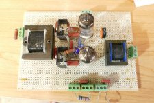
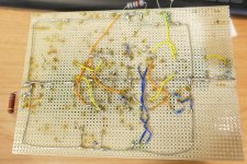
The perf board design is a completely balanced differential Voltage Controlled Amplifier for a vacuum tube music synthesizer. It uses a pair of budget Edcor transformers. Note that I ran a fat ground wire down the middle of the board from input to output. Another piece of ground wire runs around the perimeter where the power connectors are located. This works good and has very low noise even at maximum gain which is limited to about 20 Db. I would start with something close to this for the PCB layout and have a provision to ground the transformer cores to that central ground stripe if it offers an improvement.
I got a bunch of large (about 200 by 400 mm) double side copper clad board stock at a hamfest close to 40 years ago. I find it easier to make one big board with several small patterns on it. Sometimes I make one big board with several copies of the same board on it. The nice rectangular patterns make it much easier to deal with when the big board meets the table saw and the belt sander. So this has become more of a habit than a requirement. Some of my larger designs like the TSE-II do not have a border around both sides, and one of the fat traces along the back of the board is filament power to the output tubes. The filament return is ground and runs on the opposite side of the board.
Every board that I send out to a fab shop has been through my prototyping process at least once. Some, like the first TSE were done several times before I was happy with it. Early on when I didn't have any vacuum tube PC boards to look at, it was far too easy to create a board that was difficult to populate due to parts fitment issues. The pictures show the first design thar uses the UNSET output topology. It is an all on one board push pull amp with a power supply on board. It has areas especially in the center where the power supply is where the parts don't fit. The mosfets in the cathodes of the output tube needed more heat sinking than there is space on the top, so they wound up under the board. This board would need to be larger and go through a new layout and proto board round or two to be right, and it is already too large to fit in my current mailing envelopes, so the project was abandoned. Despite the ugly hacks and flying parts it does make a clean 80 WPC with the little 6GF5 output tubes. Unfortunately the 6GE5's that should go beyond 100WPC, and 6HJ5's that would get to 125 WPC do not fit in the board and were not tested.
The board in the upper right is a high gain guitar preamp board. It needs to have a full ground plane. "Leaving ground plane everywhere something else isn't," is generally a good idea and I did that on all my Motorola boards whether they involved RF or not. The Mentor Graphics boardstation software had that choice as a simple menu pick. Even there, all of the active traces, RF traces, vias, and pads for parts need to have keepout and width rules associated with them. I had automatic setups for several different kinds of boards and I never worked on anything that needed more than 32 volts for my entire career. The voltages seen in vacuum tube amps do need larger keepouts to avoid issues. The old version of Eagle pro that I use is from 2008 and cost a one time fee of $307 for the upgrade from V4.5 15 years ago. It will not do an automated ground fill, all "fills" are actually overlapping 100 mil traces and each must be done by hand one at a time. Eagle 5 is also not compatible with any of the new Eagle libraries, since the library format was changed when Newark / Farnell acquired Cadsoft. I left the tape on Mylar world when Eagle 2.5 for DOS first appeared in the early 90's. I didn't start doing boards at Motorola until I got into the research group in 1999. I have used Eagle for more board designs than any other software.
I have started down the road to learn KiCad twice but I have never actually completed a board in KiCad. If, and when I have a layout program that I fully understand that has the capabilities for a copper pour like Mentor did, most of my boards will start to look like what I made at Motorola.
Any piece of wire is resonant at some frequency. Until active electronically amplified antennas became possible, all car radio antennas were the same length. This is about the same length as the wire on a pair of headphones. This length is resonant in or near the FM broadcast band in North America (88 to 108 MHz). The headphone wire makes a good antenna for FM radio, and many pocket radios do use the headphone wire as the antenna. Cell phones operate in the 600 MHz to 2.5 GHz band, though some 400 MHz frequencies have been used in other parts of the world. A resonant wire for cell phone use would be in the 1 to 5 inch long range, so the headphone wire would be a very poor antenna for cellular without some impedance matching elements distributed along the wire. The bent paper clip that I used for GPS was trimmed with wire cutters while connected to an RF network analyzer that measured its resonant frequency.
The perf board design is a completely balanced differential Voltage Controlled Amplifier for a vacuum tube music synthesizer. It uses a pair of budget Edcor transformers. Note that I ran a fat ground wire down the middle of the board from input to output. Another piece of ground wire runs around the perimeter where the power connectors are located. This works good and has very low noise even at maximum gain which is limited to about 20 Db. I would start with something close to this for the PCB layout and have a provision to ground the transformer cores to that central ground stripe if it offers an improvement.
Attachments
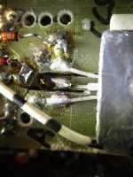
Despite all the good constructional comments; On a recent test I was bothered by a lossy capacitive problem on a CCS that made me burn the midnight oil and unnecessarily swap many CCS power transistors, when the fault lies with the PCB board.....material duff? Whatever, I decided with a Dremel and fine saw cut slots between the sensitive B and E PCB solder terminals. See pic part X. It solved the issue.
Beware when working with HV, that fiberboard leakage can be an issue, some may get away with it, but in my case it was bad example. In RF certainly it would resultin a massive loss.
Have a nice Xmas without shocks!
BB
Beware when working with HV, that fiberboard leakage can be an issue, some may get away with it, but in my case it was bad example. In RF certainly it would resultin a massive loss.
Have a nice Xmas without shocks!
BB
Attachments
Another issue that has come to light in the last few years is the ability for some solder flux residue to absorb moisture. This has been noted with "no clean flux" or "water cleanup flux."
A customer used ChipQuick water clean up solder to assemble a Tubelab SSE board which runs a B+ in the 450 volt range. After being cleaned and left in the garage to dry for a couple days the board flamed up in places where flux had been trapped around high voltage connections. One such place generated enough heat to burn and carbonize the board destroying it. That stuff may be fine on "maker boards" that operate on 5 or 12 volts. It is not suitable on a tube amp board.
Back in the late 60's and 70's it became "good practice" to run an isolation ring around the inputs of a high impedance instrumentation amplifier circuits to shield against leakage currents on the surface of a PC board.
Reading your comments on RF together with looking at your balanced differential board in post #153 has got another question going.
At some point I learned to treat ground as a buss on pretty much everything I make. First came a B+ trace/rail across the top (north) edge of the board and ground trace across the opposite - south edge (usually made with stripped wire and covered with solder to make it a fatter gauge). Then when I started building phono circuits I extended that ground up the east and west sides in a big U, thinking of it like surrounding the circuit with protective shield. . . . . But from this back and forth with you I realize I was really doing it out of a kind of faith that it would work and actually don't really understand that much about how it would (or wouldn't).
The question is , When we talk about RF noise in an audio circuit , what's the difference between a circuit creating its own oscillation at some high frequency and one resonating with RF from an external source?
This came up while looking at your board, thinking of mine, and realizing that as a shield , the ground trace only gets between the outside world and the circuit in one thin slice of an otherwise open space , so the RF I assumed I was protecting the circuit from can actually reach all the parts inside that ground loop from above or below..
I know the question is unclear but that's just it, I'm not really clear about how it works.
- Home
- Amplifiers
- Tubes / Valves
- Does audiophile tube builders know what a grid stop is for?