Why should I change C7. It seems doing the job.Have you tried changing C7 value?
It keeps the upper bandwidth to 900kHz, which is a good value.
Keeps giving a good oscilloscope wave.
This would mean changing resistor in the input as well. 6.8K is very low input impedance.I agree with bonsai. C7 is a double-edged sword.
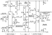
C7 is for canceling the input capacitance of U2 and must be selected so that C7/(input capacitance) = R8/R9.
If it is too large, ULGF will be postponed and it will become unstable.
Usually, it has a small capacitance of about 1p to 3pF.
I think it would be better to lower the impedance of R8, R9, and C1 further (e.g. 470Ω, 6.8kΩ, 220uF) to drive the extra pole formed by the input capacitance of U2 to higher frequencies.
I might try lower the value of C7.I agree with bonsai. C7 is a double-edged sword.
C7 is for canceling the input capacitance of U2 and must be selected so that C7/(input capacitance) = R8/R9.
If it is too large, ULGF will be postponed and it will become unstable.
Usually, it has a small capacitance of about 1p to 3pF.
I think it would be better to lower the impedance of R8, R9, and C1 further (e.g. 470Ω, 6.8kΩ, 220uF) to drive the extra pole formed by the input capacitance of U2 to higher frequencies.
1pF to 3pF.
But as it is now it works okay.
It was @minek123 that added the C7 for me.
A RED LED.I would seriously recommend that the TLV431 be replaced with a red LED. They have a forward voltage drop of 1.8V and about the same dVbe vs temp as a transistor ie -2mV/K. This will at least give the current source 1st order cancellation of output current dependency upon temperature which it does not have now (it's about 50uA/K right now, so over a 30-degree temp change, expect the current source output to shift by 1.3mA). You won't have potential TLV431 stability issues to deal with either and it's cheaper!
This is possible.
But why should I change? It works pretty wel with TLV431.
My reply was to @brian92fs , as you can see from the order of the posts. BTW, you have no oscilloscope wave. You have a simulator wave. That is a big, big difference. You do not know how the real amplifier would behave.Why should I change C7. It seems doing the job.
It keeps the upper bandwidth to 900kHz, which is a good value.
Keeps giving a good oscilloscope wave.

Hitachi's laterals and their second sources have a Q point at which the temperature coefficient becomes 0 at around 120mA, so many DIYers set the value around that.Is 200mA a good value in the output or should I decrease it a bit?
For FETs with square-law characteristics, the larger the bias current, the lower the distortion. At 200mA, the temperature coefficient is negative, so as long as the heat dissipation conditions are acceptable, there should be no problem.
However, the temperature coefficient is negative when the bias voltage is constant. In this circuit, the bias circuit is not a constant voltage circuit but just a resistor, so it changes in proportion to the quiescent current of the VAS.But why should I change? It works pretty wel with TLV431.
It is recommended that the temperature coefficient of the VAS current is also close to 0 according to the advice of Bonsai.
Since the temperature coefficient of TLV431 is 0, it cannot cancel the temperature coefficient of U7.
Last edited:
Of course you are very right.My reply was to @brian92fs , as you can see from the order of the posts. BTW, you have no oscilloscope wave. You have a simulator wave. That is a big, big difference. You do not know how the real amplifier would behave.
Simulations are one thing - real amplifier a whole lot of different.
It is just that I have no real amplifier - so I have to use simulations.

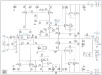
For the RC caps R14 & R15, I don't think they need to be this high. I'd suggest dropping from 4700u to 470u. PSRR will still be good and PCB layout will be easier. 4700u caps can get quite larger.
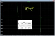
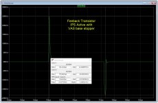
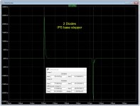
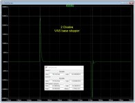
For the IPS & VAS CCS, I ran some simulations on different configuration to see how it impacts slew rate. I tested 2 diode and feedback transistor style CCSs with the base stopper at the VAS or IPS side.
You can see that placing the base stopper on the IPS side improves negative slew rate and the feedback transistor version performs slightly better.
These sims were all ran with 20V rails with a 20KHz square wave at 1V peak
You can see that placing the base stopper on the IPS side improves negative slew rate and the feedback transistor version performs slightly better.
These sims were all ran with 20V rails with a 20KHz square wave at 1V peak
Attachments

Yes and not only. 4700uF on-board bypass capacitors are a source of current peaks that flow through the PCB ground tracks and as a result there is a raise of mains component multiples at the amp output. Just the opposite than the author wanted to have. Again, it is necessary to build prototypes to know this. Or to make much more complex simulations.For the RC caps R14 & R15, I don't think they need to be this high. I'd suggest dropping from 4700u to 470u. PSRR will still be good and PCB layout will be easier. 4700u caps can get quite larger.
I cant test those, I think.How are phase margin and gain margin values now?
What I test is only AC Analysis and Fourier Analysis.
And simulation Oscilloscope
Thanks.For the IPS & VAS CCS, I ran some simulations on different configuration to see how it impacts slew rate. I tested 2 diode and feedback transistor style CCSs with the base stopper at the VAS or IPS side.
You can see that placing the base stopper on the IPS side improves negative slew rate and the feedback transistor version performs slightly better.
These sims were all ran with 20V rails with a 20KHz square wave at 1V peak
See the image.
Self uses IPS base stopper in his Blameless. And two diodes CCS..
Attachments
I will make them 1000uF. They are not big.For the RC caps R14 & R15, I don't think they need to be this high. I'd suggest dropping from 4700u to 470u. PSRR will still be good and PCB layout will be easier. 4700u caps can get quite larger.
And @PMA gives another reason not to use very large capacitors.


Self uses IPS base stopper in his Blameless. And two diodes CCS..
For the blameless PCB he sells, he uses the feedback transistor version. With the VAS as the active device and the base stopper on the IPS side.
Attachments
@brian92fs
I ran oscilloscope square and tested making C7 2pF. Not perfect square at 10kHz.
3pF was better, okay.
I think 5pF is on the safe side.
I ran oscilloscope square and tested making C7 2pF. Not perfect square at 10kHz.
3pF was better, okay.
I think 5pF is on the safe side.
- Home
- Amplifiers
- Solid State
- Cello One. Good Amplifier 15 Watt with TMC and Laterals