Mosfets do not have emitters 🙂
Since he is using lateral mosfets, source resistors are not necessary because for one there are no parallel pairs to balance and two the thermal characteristics of that technology do not have a thermal run away problem as would a bjt or other mosfet type such as a hex fet
Since he is using lateral mosfets, source resistors are not necessary because for one there are no parallel pairs to balance and two the thermal characteristics of that technology do not have a thermal run away problem as would a bjt or other mosfet type such as a hex fet

I dont think there would be a point in using an emitter resistor in the VAS in this case? Thinking it would just worsen the gain of the PNP common emitter.
Is there anyone who builds this amp with PCB by prasi?
Until now .... I have built dac, preamp and poweramps with shared BOM having mouser parts.
I purchased LSK170 quad from diyaudio store and EXICON mosfets from profusion.
Is there anyone to help fill out correct or proper mouser parts on this doc (latest shared by prasi)
Until now .... I have built dac, preamp and poweramps with shared BOM having mouser parts.
I purchased LSK170 quad from diyaudio store and EXICON mosfets from profusion.
Is there anyone to help fill out correct or proper mouser parts on this doc (latest shared by prasi)
Attachments
Hi namghiwook,
I dont have pcb, may be someone who ordered the pcb as per post # 90 help you to get pcbs.
here is the parts list with mouser part numbers as a guide.
i have selected those parts that have large stock and cheaper. you may go for premium /costly parts if you wish.
hope this helps.
regards
prasi
I dont have pcb, may be someone who ordered the pcb as per post # 90 help you to get pcbs.
here is the parts list with mouser part numbers as a guide.
i have selected those parts that have large stock and cheaper. you may go for premium /costly parts if you wish.
hope this helps.
regards
prasi
Attachments
Yes, the gerber file in the zipped file in post #90 works fine - ordered at JLCPCB and they were delivered here yesterday.
On the list to build.
On the list to build.
My 2 cents on compensation:
Do connect c5(22p) with the gates/bases of power transistors instead of output. In many cases this increases stability considerably.
Just the way I did it with my first 2x500W latFET amp, published 1985
Do connect c5(22p) with the gates/bases of power transistors instead of output. In many cases this increases stability considerably.
Just the way I did it with my first 2x500W latFET amp, published 1985
Attachments
Last edited:
Does the IDSS of the J113 need to be anything in particular (~4.5mA) or just matched? I have ranges from 3ish to a little over 9mA.
PCBs in my hands now, hope to start dropping parts in soon!
Interested to hear if anyone has any progress with theirs.
PCBs in my hands now, hope to start dropping parts in soon!
Interested to hear if anyone has any progress with theirs.
Do you have a high resolution image of schematic and also any suggestions for substitutions for obsolete partsMy 2 cents on compensation:
Do connect c5(22p) with the gates/bases of power transistors instead of output. In many cases this increases stability considerably.
Just the way I did it with my first 2x500W latFET amp, published 1985
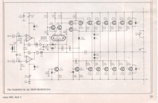
Sorry if this was answered already.The name of this amplifier is EXIAMP10.
Because the output devices are EXICON transistors and the target power is 10 Watt Class A.
The input is a quality JFET: LSK170.
I will test this amplifier in simulation. Also use a simulation oscilloscope.
AC Analysis and Fourier Analysis are also possible.
View attachment 1210632
Which Idss grade 2SK170?
GR OR BL?
Sorry, but I cannot give more support to this itemDo you have a high resolution image of schematic and also any suggestions for substitutions for obsolete parts
Wonder if anyone has made progress on this yet?
I've done the boards (need to tidy up the heatshrink on the inductors and add LEDs still).
I haven't got a suitable transformer on hand, so I'll have to wait until I get one before I can see if this makes noise.. or smoke..

I've done the boards (need to tidy up the heatshrink on the inductors and add LEDs still).
I haven't got a suitable transformer on hand, so I'll have to wait until I get one before I can see if this makes noise.. or smoke..
Does anyone know what the typical real gate leakage current is for the double die latfets in this application? It doesn't seem to be in the model. (If it is then it's accommodatingly small.) I'd be tempted to try a photovoltaic optocoupler bias voltage generator like TLP3905 or two and get another couple few peak drive volts closer to the rail.
Last edited:
Does that use a transnova output configuration? I wonder how the OPer circuit would fair in transnova.My 2 cents on compensation:
Do connect c5(22p) with the gates/bases of power transistors instead of output. In many cases this increases stability considerably.
Just the way I did it with my first 2x500W latFET amp, published 1985
- Home
- Amplifiers
- Solid State
- Scope Design: JFET Input EXICON Output 10 Watt Class A