Stef,
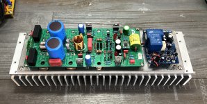
Reflow ALL solder joints on your psu board. Insufficient solder and cold joints are visible in the picture, especially those faston tabs. Try that first 😉
Reflow ALL solder joints on your psu board. Insufficient solder and cold joints are visible in the picture, especially those faston tabs. Try that first 😉
I gave a little bit of welding but it's the photo that gives this impression. There was already a good layer of solder below and above.
No change. It crackles when I plug in but I can't find what exactly makes the noise. It seems to come from within one of the capacitor, but it's hard to tell which one. I've 53v at out as usual. As I don't want the 10000uF to explode in my head, I don't dare leave it on for more than a few seconds.
I will end up finding it.
Stef.

Good evening,
I've found. I just had a FASTON terminal at input which was tight enough. Must say that it was a test power supply and I spend my time disassembling it.
Saligny bridges seem to work well. I have 53Vdc with 240Vac input and a 2x35v toroid.
To be continued...
Stef.
I've found. I just had a FASTON terminal at input which was tight enough. Must say that it was a test power supply and I spend my time disassembling it.
Saligny bridges seem to work well. I have 53Vdc with 240Vac input and a 2x35v toroid.
To be continued...
Stef.
I have a technical question concerning the output transistor matching. Tibi says they shall be matched for Vgsth and transconductance (#1711).
Stef uploaded a setup for matching the output MOSFETs under #1526, which also appears in some of the white papers published by NP. As I understand, this setup - although it does not measure Vgsth directly at Id~170mA, is still a good tool to judge the latter: As long as the measured Vds are close for two transistors, their Vgsth values cannot be very different, either. Question Nr. 1: Is this argument correct?
Question Nr. 2: Can you please propose a practical setup to measure the transconductance? I think the difficulty lies in the fact that at affordable test currents, Id of the FQA is far from saturation. Therefore, when Vgs is increased, Id increases. However, assuming a constant bias on the transistor + series resistor circuit, a higher Id will increase the voltage drop on the resistor, which means that Vds of the transistor has to decrease. Since we are not yet in saturation, a lower Vds reduces Id. This results in a systematical error in the transconductance calculation. Of course, one can measure Vds independently and keep it constant by adjusting the bias when changing Vgs. But I wonder if there is a simpler and smarter method in your magic box.
Thanks,
Miklos
p.s. Stef: I am not yet at the Q17 build but I just ordered PCBs from JLCPCB for another project - plus your external pcb coil v1.1. This means an important step toward the impedance measurements which I promised a while ago. ;-)
It is true that if you use several pairs, you have to measure and match the output MosFet.
I do this with my Peak DCA75Pro, which allows me to sort the components according to characteristic curves, which is sufficiently accurate for me.
But there is still no electrotechnical reason for me to build a double pair of mosfet with source resistor, because this design has a lower amplifier damping factor due to the resistors and because of the performance of the mosfet I don't get distortions at high power with one pair.
So two pairs need to be measured out, tend to have higher distortion values according to Stef's measurements and lower speaker damping....
Why do you do it?
So far, even with the 500W power supply, I have not been able to get only a single output stage to distort audibly, nor have I overloaded any component. I have not reduced the amplification factor of the circuit and my DAC supplies approx. 1.4V output.
Explain to me what the point is.
Regards Tim
A1: I will build and listen to both the single and double output version and decide which one I prefer sound-wise.Explain to me what the point is.
A2: Following Tibi's recommendation under #1720, I will start with the double-pair version.
Any thoughts on proper transconductance measurements beyond "hoke up your transistor to a black box"?
Thanks,
Miklos
Hi Miklos,
I like that you compare several variants, maybe there are new findings. Do you use the same type of PCB for both variants?
I like that you compare several variants, maybe there are new findings. Do you use the same type of PCB for both variants?
Hi Tim, yes, this is precisely the idea: Preferably one change at a time for the sake of conclusiveness. 🙂 Back to matching: even for the single pair version, closer Vgsth and transconductance between the P and N MOSFETs as well as between the two boards is probably a good thing. Since I will have all my output transistors measured anyway, I would definitely go for the closest match even for the single pair version.
Fundamentally correct. However, the amplifier works completely unbalanced, so the primary goal is the tight selection of the individual duos, which should theoretically work identically. Therefore, a measurement is not necessary when setting up the Signle pair variant.
Hello,
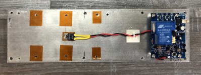
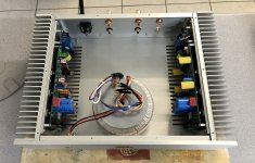
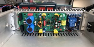
The amp has advanced a bit this weekend. I'm missing a few screws to complete the integration of the board in the chassis. The transformer is a TALEMA 2x40Vac 500W. It gives 60/61Vdc loaded.
Regards,
Stef.
The amp has advanced a bit this weekend. I'm missing a few screws to complete the integration of the board in the chassis. The transformer is a TALEMA 2x40Vac 500W. It gives 60/61Vdc loaded.
Regards,
Stef.
Attachments
And There you go !!
Q5 : FQP3P20, FQP3P50 or IRF610
Q6 : FQP3N30, FQP3N50C or IRF9610
Q15 : FQA46N15, IXFH50N85X or IRFP240
Q16 : FQA36P15, IXTH48P20P or IRFP9240
Q5 : FQP3P20, FQP3P50 or IRF610
Q6 : FQP3N30, FQP3N50C or IRF9610
Q15 : FQA46N15, IXFH50N85X or IRFP240
Q16 : FQA36P15, IXTH48P20P or IRFP9240
See:Hi
What mosfets can I replace
FQP3P20&FQP3N30
Which I can't find
Thank
https://www.diyaudio.com/community/...approach-to-perfect-sound.374507/post-7383991
HI
And thanks
I already have a quad 405 clone.
I want to try building Q17 to see the differences
Thanks to you all
And thanks
I already have a quad 405 clone.
I want to try building Q17 to see the differences
Thanks to you all
@stef1777 I got your mini 1.3.1 boards printed and wanted to build this as a summer amp and put my SIT amp to rest till the winter. As I have good sensitive speakers Klipsch Forte III I just need few watts, so I do have a spared Antek 24vac dual secondary 400VA transformer to go with it? Gets me close to 31-33vdc rectified without load. I hope this is good enough and I can expect to get around 20-30wpc out of this amp.
Let me know if its good to go.
Thanks
Let me know if its good to go.
Thanks
Hello,
Ellers look very sympathetic to these Klipsch Forte speakers. It still has a 30cm boomer and it probably takes current to power them even if they have good sensitive.
The Q17 should operate at 31vDC. From memory, the board starts running at 29v. It's still not ideal to operate so close to the low limit.
I also seem to remember that it will be necessary to change the value of R25 (default 7k5) but I forgot the value for 30v.
Regards,
Stephane
Now I was thinking of getting a SMPS rather than a new toroidal like this with +/-55vdc - https://connexelectronic.com/product/smps300reh/
Hopefully enough wattage for this amp.
Hopefully enough wattage for this amp.
You can try it out and write how well you hear the noise and whistle of the switching power supply. Your Klipsch speakers will play it for you in detail.
I have a friend who uses the Q17 only for shelf speakers, so also for higher volume and his Q17 has a Japanese transformer with 2×25 V AC and 50VA.
Compared to the Q17 with 300VA with the same speakers you don't hear any difference.
Therefore:
A high capacitance on the rectifier board (40,000uF) can also compensate an undersized transformer.
- Home
- Amplifiers
- Solid State
- Q17 - an audiophile approach to perfect sound