@grunf Right, I see in the AD797 datasheet that 1k is the highest (unfiltered) input resistor recommended for low noise.
I’ve been able to remove the AD797 oscillations under load in my prototype SR circuit by shunting its power supply pins with a low ESR 100u cap. So now I’m building the final real circuit with AD797 and need to know the best values for the input resistors. On Jan’s diagram, it is 500R on the non-inverting input and a 1k-filtered/1k voltage divider on the inverting input.
Assuming I will use the lowest leakage polymer caps, what resistor/capacitor values would you recommend for R4, R6, R7 and C8, C3? Should I increase R4 to 1k (since it is filtered) and C9 to 330u? Should I decrease R6 and R7 to 500R? And what about C3? Thanks so much for your insight!
@safesphere The problem is not in the noise but in the error at the output of the regulator, for the AD797 I would stick to the value from the original scheme, especially since the AD797 tends to oscillate in this application. The ADA4625-1 is a great replacement for the AD797 and it's also a jfet op amp that allows Walt's upgrade to be used.
Yes, I don't see the point in insisting to use the AD797 when Walt and Jan, the original designers, had so much problem to tame it and in the end didn't recommend using it.
Ref #3,015/ #3,018
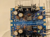
1.3k now fitted to R6/13
discovered led's installed incorrectly, replaced with new in correct orientation, Neg LED now illuminated..
Zeners all installed correctly,
Voltages
D7 12.1, D8 .2, D9 .2, D2 1.4, D3 .25, D4 .25.
LED Pos 1.4, Neg 1.9.
Op Amp
Leg 2/3 .2, Leg 4/7 27.5.
voltages are 28.5v input to superreg
27.5v pos out
15.7 neg out
What are the voltages on D5/D10? Also, are the outputs connected to the senses? On Jan’s 2.3 diagram, the pins of J2 should be connected 1 to 2 and 3 to 4. Also similarly the pins of J6 also should be connected 1 to 2 and 3to 4.
To make sure my statement is clear, do NOT connect any J2 pins to any J6 pins. The connections should be like this:
J2:
1-2
3-4
J6:
1-2
3-4
The voltage on D2 is incorrect. It should be 12V. Check the polarity of this zener again. Note that the polarity if this zener is different between the positive and negative regulators. This however may be only a symptom of the opamp inputs being out of range.
Last edited:
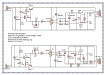
The part numbers are those from Jan Didden's latest circuit in Linear Audio?Ref #3,015/ #3,018
1.3k now fitted to R6/13
discovered led's installed incorrectly, replaced with new in correct orientation, Neg LED now illuminated..
Zeners all installed correctly,
Voltages
D7 12.1, D8 .2, D9 .2, D2 1.4, D3 .25, D4 .25.
LED Pos 1.4, Neg 1.9.
Op Amp
Leg 2/3 .2, Leg 4/7 27.5.
voltages are 28.5v input to superreg
27.5v pos out
15.7 neg out
"Safesphere"
Links to J2/J6 fitted,
output now 24.2v pos, 24.2v Neg.
D5/D10 9.9v (i suspect that this is now academic)
Safesphere, Thank you very much for persevering with me, I can now move on to connect to my BA3 Fe.
Once again Many Many Thanks
Links to J2/J6 fitted,
output now 24.2v pos, 24.2v Neg.
D5/D10 9.9v (i suspect that this is now academic)
Safesphere, Thank you very much for persevering with me, I can now move on to connect to my BA3 Fe.
Once again Many Many Thanks
@esprit
It will work with these links, but the sound quality will improve if you remove the links at the J2/J6, run all 4 wires from each output to the load, and connect the same wires at the load instead of connecting them at J2/J6. I use twisted pairs: 1 and 4 is one pair, 2 and 3 is another pair. The latter pair (2 and 3) ideally should be shielded and the shield grounded, but it should work even without the shield.
It will work with these links, but the sound quality will improve if you remove the links at the J2/J6, run all 4 wires from each output to the load, and connect the same wires at the load instead of connecting them at J2/J6. I use twisted pairs: 1 and 4 is one pair, 2 and 3 is another pair. The latter pair (2 and 3) ideally should be shielded and the shield grounded, but it should work even without the shield.
Which ground would you recommend for the shield?The latter pair (2 and 3) ideally should be shielded and the shield grounded, but it should work even without the shield.
On my application, which is replacing shared 317/337 on one preamp, and series 7818 + 7815 and 7918 +7915 regulators on the other, I will not have space for separate SRs for each channel. I would have to share the SRs on both channels. As I am not handy with SMD parts that is not an option either.
I haven't yet seen, on the pcb design, how small can I get putting resistors and diodes standing up, but I am not too optimistic. If anyone knows some existing design using such technique, please let me know.
I haven't yet seen, on the pcb design, how small can I get putting resistors and diodes standing up, but I am not too optimistic. If anyone knows some existing design using such technique, please let me know.
Which ground would you recommend for the shield?
According to this article, the screen should be grounded only on one end at the Super Regulator by connecting to the sense ground, pin 3 of J2/J6.:
https://linearaudio.nl/sites/linearaudio.net/files/Regs_for_High_Perf_Audio_3.pdf
I will not have space for separate SRs for each channel. I would have to share the SRs on both channels.
I am not an expert, but I can think of only two reasons against sharing a SR: (1) the current demand is higher than what one SR can supply and (2) the channels don't have a common ground.
I am sorry that there was a zenner diode with Japanese letter product label included in my photo.
So I post again.
I would like to have advice.
I built +/-5v super reg but negative rail has only -4v output.
I checked resistors again but couldn't find my mistake.
I use 5K for R1,R8
910 for R6,R13
1k for R7,R14
2.5v zener for D2,D7
Q2=BC556C Q4=BC546C
AD817
So I post again.
I would like to have advice.
I built +/-5v super reg but negative rail has only -4v output.
I checked resistors again but couldn't find my mistake.
I use 5K for R1,R8
910 for R6,R13
1k for R7,R14
2.5v zener for D2,D7
Q2=BC556C Q4=BC546C
AD817
Attachments

Thank you for help
DC input is 12v,I don't have scope.
I put 3.3k for dummy but output is still +5v-4v.
Checked opamp between 2pin and 3pin.
Pos 0.55v,Neg0.54v
DC input is 12v,I don't have scope.
I put 3.3k for dummy but output is still +5v-4v.
Checked opamp between 2pin and 3pin.
Pos 0.55v,Neg0.54v
What are the voltages between the opamp pin 2 and the ground and between the opamp pin 3 and the ground on the negative side?
- Home
- The diyAudio Store
- Super Regulator