This reminds me of smartphone cameras which are mass produced items for a few dollars.
Of course the lens is crap, even though they paid money to have them "certified" by some famous European optics company.
The image "quality" is all done by a calibration and then software correction, given enough resolution.
Ask a German lens designer for professional cameras what they think.
(And I happen to know the answer.)
Of course you cannot expect anything else from a smartphone.
But hi-end audio ?
🙂
Patrick
Sawyers et al,
Wow, I'm in "august (augustus)" company here. Most of you'se guys are what I will coin PROFESSIONAL DIY'ers. Versus rank AMATEURS like me. You who have agilely switched to SMD parts that I can't even see.
In my previous post - referring to the death of thru-hole's, I'm lamenting the result on the amateur's or especially newbies trying their hand at accumulating solder burns. No more "breadboarding", "dead bug" or whatever more modern terms. If you're old like me, we're stuck with dusty parts bins stocked with many obsolete things like 709 IC's, tube sockets and solder strips??? AN OHMITE RESISTOR CHEST!!!???? OMG
And my take from following DIY postings over the years show that many/most? new DIY'ers are adept at MODELING stuff - but actually building anything???
Any of you able to solder with either hand??? "ambi-solderous?"
I'm reasonably solidly right handed - so iron in one hand and solder in the other. But yes - how do people new to this stuff get "practical" experience? Us old lags have gone from AB carbon composition resistors that were big enough to read the colour code, to modern tiny ones with umpteen bands that I have to use a magnifying glass to read, and then a final check by meter. Faced with bands that read different values depending on what end you read from, a meter check is kind of essential
The thing that gets me about surface mount is that capacitors have no identifying information at all on them. Ceramic could be either X7R or COG and who can tell what value. No way to tell unless you have a measurement bridge with a surface mount fixture and look at value and D. Resistors are OK for printed values in the same format as Dale resistors, but if you lose track of which are thin film and which are thick you are absolutely sunk.
Most opamps are now only in SM - either SOIC which is pretty straightforward to solder to TSSOP with very small pin pitch and is more tricky. And bump mounted - forget it. I actually had to look up what TSSOP was an acronym for - Thin Shrink Small Outline Package. Who thought of that unpronounceable acronym?
But the only way to do this is to model it, and then commit to board manufacture. I get mine from China.
But the days of quick and dirty lash ups are fading fast. Back when I was a kid, I used to build stuff on Formica, drilling holes with a needle I'd blunted for the purpose, putting the component leads through and soldering on the back of the board. And its a bit like the Monty Python sketch "But you try and tell the young people today that... and they won't believe ya"
That is very interesting Mark. The specification is a little foggy - it is not clear if it measures D too.
Actually I have a number of high precision bridges that do C and D already. I just need to work up a fixture.
Actually I have a number of high precision bridges that do C and D already. I just need to work up a fixture.
There is certainly a whole range of possibilities Thor. My good friend and mentor Gordon Edge (RIP) challenged thinking about technology, business and spin out companies. He was the founder of Cambridge Audio in the 1960's - but was very active in pushing for exactly the technology you are talking about - but thirty odd years ago - and entirely digital environment. The killer is always at the end of the chain - the loudspeaker/headphone - which is always analog. If a truly "digital loudspeaker" were possible, that would close the whole digital chain.
Something currently waiting to be revived (investment) is exactly that. Fully digital system to the voice coil. Fully active. Naturally digital in, plus ADC if requiring an analogue in. All the things I wrote up above included. And yes, prototypes did sound rather "Audiophile", unless the DSP was reprogrammed for "Just Brutally Loud".
I did first theorise about such systems in the mid 90's on the then "Bass List", that would have been just around when the internet came out. Now I can realise them and there seems little interest.
Thor
The first disclosure of a class D audio amp was in 1963 "Modulated Pulse Amplifiers" in https://worldradiohistory.com/UK/Wireless-World/60s/Wireless-World-1963-02.pdf . This was developed into a product by Gordon Edge for Sinclair in 1964 - the X10. This had been designed as a 2.5W amplifier. Now 2.5W average power is 5W peak, which is what Sinclair latched onto, believing it was the average power - so he doubled it again to 10W, whereas the real-world average power was 2.5W. That was typical Sinclair - over sell and under perform.
This is what it looked like (along with some of Sinclair's other products) https://www.audiosciencereview.com/forum/index.php?threads/class-d-pwm-amplifier-archaeology.37017/
Things have moved on just a bit since then!
This is what it looked like (along with some of Sinclair's other products) https://www.audiosciencereview.com/forum/index.php?threads/class-d-pwm-amplifier-archaeology.37017/
Things have moved on just a bit since then!
tweezer LCR meter .... smart .... I need one of those 😉Get a tweezer LCR meter. Amazon sells the LCR-58 for USD 105 and there are other models by other manufacturers which cost more.
One her even cheaper ... https://www.electromaker.io/shop/pr...nUXU3ZFCZfapJuJ85MFQYJheqYVL7HyXbBsa3rtgih_k4
I have also invested in a fair priced digital PC microscope ..... good for many things, e.g. checking smd solderings 😉
(same as this one: https://www.bhphotovideo.com/c/prod...JkJf-ZVKntwO5uDecpyV1OTvJSz4phVGxU5zPQUbIaiWc)
Last edited:
The first disclosure of a class D audio amp was in 1963 "Modulated Pulse Amplifiers" in https://worldradiohistory.com/UK/Wireless-World/60s/Wireless-World-1963-02.pdf .
I am familiar with this via reporting in the contemporary east german RFE. The original was criticised somewhat on the basis of the 50kHz carrier frequency.
I did not realise (make the connection) it was invented by David Birt of the BBC, who is usually associated with other circuitry, especially in balanced line receivers.
On the other hand it was staff at Royal Philips that realised that actually a class D amplifier is just an audio modulated buck switching converter.
That was typical Sinclair - over sell and under perform.
Yeah, sounds like him. Good salesman.
Things have moved on just a bit since then!
Indeed, though I still find the State Of The Art disappointing.
Having grown up with RF, military and industrial systems as well as audio, it is easy to see simple solution to the various problems that plague the best Class D amplifier and seemingly invariably are fixed by more loop feedback, instead of solving the root cause.
Thor

Have you come across Halcro? Originally founded by a guy called Bruce Candy, whose main business was is professional metal detection. The story is here, https://halcro.com/history/ . Basically a power factor corrected switched mode supply, and then an amplifier whose topology is shrouded somewhat in mystery, but might possibly be disclosed in US patent 5892398A . The amp was specified to be sub ppm distortion over the whole audio band at full power. Something John Atkin's Audio Precision test gear and load struggled with. It took Candy's assistance to point out how to measure the amp, resulting in distortion below the AP noise floor up to clipping, load independent.
Because, as you know by now I cannot leave things alone, I have put the entire schematic of Burwen's op-amp prototype for the Audio Palette into Spice. It is surprisingly good.
With 6Vrms into the input, and bearing in mind the number of stages the signal goes through, and the balanced output loaded with 600 ohms, it returns:
Output noise 13uV 20Hz to 20kHz or a S/N ratio of 97.5dB unweighted (or over 100dB A-weighted). and 0.00017% THD (1.7ppm). Achieving that performance in practice would need exceptional care with board layout, particularly power supply and ground routing.
Burwen certainly knew what he was doing when he designed it! I'd love to see his prototype.
Steve "Apple" Wozniak soldered with his mouth. YouTubeAny of you able to solder with either hand??? "ambi-solderous?"
If a truly "digital loudspeaker" were possible

OK - if you want red book 16 bit as your base standard, that involves radiating areas between MSB and LSB in the ratio ~66,000:1 (2^16). A pretty tough ask.
Three or four bits, possibly. 16 bits not a snowball's chance. And by the time you get to 24 bit - area ratio of 16 million:1?
Three or four bits, possibly. 16 bits not a snowball's chance. And by the time you get to 24 bit - area ratio of 16 million:1?
Have you come across Halcro?
Yes. They were all the rage for a while. Heard them with a few speakers I liked, they sounded ok. Heard them on speakers I hated, they did not rescue them.
There were many guesses on the insides. No pictures circulated and Halcro played their cards quite close to their proverbial chests.
They kinda faded away. Haven't heard the name in years.
Originally founded by a guy called Bruce Candy, whose main business was is professional metal detection. The story is here, https://halcro.com/history/ . Basically a power factor corrected switched mode supply, and then an amplifier whose topology is shrouded somewhat in mystery, but might possibly be disclosed in US patent 5892398A .
The Amp in this patent is actually, AFIACT a variation on the "Lavardin" topology. Heavily cascoding of all stages, many compound feedback pairs. High open loop gain and feedback overall. It could likely do sub ppm THD, though I wonder what the particular point would be, other than "we can".
The amp was specified to be sub ppm distortion over the whole audio band at full power.
Not impossible. 1ppm is only -120dB and we do better than that in headphone Amp's all the time. Harder for Speaker Amplifiers, but all it needs are big heatsinks and many output pairs or VERY BIG switching fets, maybe even IGBT. Seeing the size of the fairly modest power monoblocks and seeing the PSU is SMPS, it seems entirely possible.
Thor
The other way of squaring the ultralow distortion circle is a combination of feedback and feedforward. Stochino showed a design process and overall design in a series in Linear Audio. The real difficulty getting a design using those principles stable, and not an oscillator. Device choice and layout is absolutely key to avoid the whole raft of layout based distortions that Doug Self sets out.
Of course the good old Quad 405 in the mid 70s used feedforward to correct for distortion when the current dumpers kicked in (although they did not describe it as such), and the current generation of Quad non-valved/tubed power amps still use dumping.
Craig
Of course the good old Quad 405 in the mid 70s used feedforward to correct for distortion when the current dumpers kicked in (although they did not describe it as such), and the current generation of Quad non-valved/tubed power amps still use dumping.
Craig
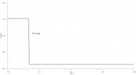
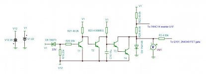
As part of understanding some of the subtleties of Burwen's design, I set to get to grips with the turn on delay to let the thing wake up before connecting the signal feeding the output drivers. The schematic is attached along with the two key signals.
V12 is the unregulated incoming -28V line, and V1 is the regulated +22V line.
T1 and T2 and associated circuit are to ensure that C16 is initially discharged. After which C16 charges up via R23. That only needs to charge by 1.2V (the two Vbe drops of the Darlington pair T3/T4). The switching time is C x (2Vbe)/I . Now I is set by 4.99M resistor R23. That has V12+V1 = 50V across it, and so passed 10uA. So the predicted switching time is 1.8 seconds. Simulation gives 1.7 seconds, so good agreement.
That is at odds with Burwen's description which says a 5 second delay. Obviously by increasing R23 or C16 you can set whatever delay you want. 47u instead of 15u gives close to 5 second delay.
One output feeds the FET clamp. That goes from ~0.6V (set by D9, and switching the FET hard on) to close to -28V to turn it hard off. Since the 2N4340 FET has a Vgs(max) of -50V that negative drive voltage is fine.
There is also a line that goes to a logic inverter (that feeds a CMOS analog switch). I chased my tail for a while, because, as you can see from the signal, it goes from +11.3V to -2.7V - surely way outside TTL logic levels. However, again Burwen subtlety, the 49.9k resistors R22 and R24 limit the current into the protection diode clamps in the logic inverter. These are specified at +/-20mA max for HC TTL. R22 and R24 limit that current to +400uA and -88uA, so well within the specified limit, and the inverter operates perfectly.
Attachments

Last edited:
That is a bit of a statement I think 😉 ....... what problems, and what easy solutions?Having grown up with RF, military and industrial systems as well as audio, it is easy to see simple solution to the various problems that plague the best Class D amplifier and seemingly invariably are fixed by more loop feedback, instead of solving the root cause.
Thor
Though agree, that it seems that there is a race for achieving the lowest THD and much of the medicine is fb (a bit like the 70's)
That is a bit of a statement I think 😉 ....... what problems, and what easy solutions?
Problems?
Ok. Give you an example.
Output filters cause problems. Enclosing them in a feedback loop helps audio band frequency response variations, but makes fixed frequency designs (clock locked to a digital input) difficult.
Worse, common output filters leak a lot of of the switching / carrier frequency. I will use "Carrier" from here-on, as this will make it easier for RF people to catch on.
Let's have a 400kHz switching amplifier with 100W/8Ohm and a 40kHz -3dB point for our output filter, a critically damped 2nd order lowpass. We will already see more than 1dB attenuation at 20kHz and our carrier attenuation will be 40dB. With a 80V PP carrier we see 0.8V carrier from a low source impedance.
But actually our self oscillating amplifier varies switching frequency with level, delivering rated power will likely leave us with 160kHz or so switching frequency, meaning our filter now filters only 24dB, so 80V PP become ~ 4V PP across the load, from a low impedance.
It certainly means using an AP2 to test such a class D amplifier shows huge THD & N that is highly variable with signal. But we just use an AUX-0025 filter and we no longer "see" this carrier leakage. And out of sight is out of mind and out of mind does not exist. Anyway, even if our speaker could respond to (say) 160kHz no listener could hear it, right?
Not so fast. Ferrite cored output inductors add distortion because of hysteresis. It was recently "discovered" by a Famous class D amplifier designer who "solved it by adding more negative feedback.
And yes, the core nonlinearities give rise to intermodulation between carrier and signal. And adding a lot of extra feedback around this will not really solve this. Worse, as the IM frequency is signal variable we will not see the result in a heavily averaged FFT, we would only see this with a fixed carrier.
But hey, it should not matter anyway, right?
Depends.
Let's look at a typical tweeter. It is a coil wound around a solid steel core. This gives rise to eddy current distortion, that is cubic functions with level and frequency. Given the level of carrier breakthrough into this nonlinear system with music is likely much higher than actual signal levels, audible results percieved as fidelity impairment are possible.
ANY linear Amplifier, even underbiased class AB will be from this impairment and the impairment cannot be directly determined testing only the individual device, but must be tested in the system.
A test could look at the current in the voice coil of a suitable tweeter with crossover, as current in the voice coil is a directl proxy of the force driving the diaphragm. The acoustic output cannot be lower distortion than this, excluding cancellation effects (which lower THD but tends to raise individual harmonics).
Though agree, that it seems that there is a race for achieving the lowest THD and much of the medicine is fb (a bit like the 70's)
I do not consider "lowest THD" as a valid design goal. There is no proven correlation between low (lower than needed to be inaudible) THD and perceived "good sound" or a perception of "reduced fidelity impairment" or a perception of "improved fidelity". Thus it is pointless.
It reminds me of the old story of the drunk guy apparently looking for something under a streetlight. When the Cop asks him he tells the cop he is looking for his house keys.
The Cop helps looking, after a few minutes the cop ask: "Are you sure you lost the keys here?".
The drunk guy points somewhere into the darkness and says: "No. I lost them over there!".
The Cop asks: "Then why are you looking here?".
The drunk guy replies: "The light is better is here, easier to search!".
Thor
There is also a line that goes to a logic inverter (that feeds a CMOS analog switch). I chased my tail for a while, because, as you can see from the signal, it goes from +11.3V to -2.7V - surely way outside TTL logic levels.
The logic used is CMOS not TTL.
However, again Burwen subtlety, the 49.9k resistors R22 and R24 limit the current into the protection diode clamps in the logic inverter. These are specified at +/-20mA max for HC TTL. R22 and R24 limit that current to +400uA and -88uA, so well within the specified limit, and the inverter operates perfectly.
I do similar things all the time. I use logic gates as clipping detectors for Class D Amplifiers working that way. Engineers of Burwen's generations still understood what happens inside IC's and how this may be used to simplify or improve circuitry.
Thor
Yes it is indeed CMOS not TTL. But the +/-20mA input current limit still applies, so the 49k9 resistors still limit input current to a hundred uA or so.The logic used is CMOS not TTL.
Thor
Last edited:
- Home
- Source & Line
- Analog Line Level
- Cello Palette Style EQ Design (was High End Tone Control)...