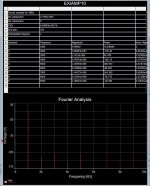
The name of this amplifier is EXIAMP10.
Because the output devices are EXICON transistors and the target power is 10 Watt Class A.
The input is a quality JFET: LSK170.
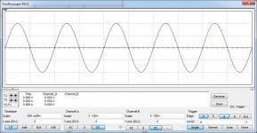
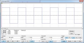
I will test this amplifier in simulation. Also use a simulation oscilloscope.
AC Analysis and Fourier Analysis are also possible.
Post #85 and further there is a PCB.

Because the output devices are EXICON transistors and the target power is 10 Watt Class A.
The input is a quality JFET: LSK170.
I will test this amplifier in simulation. Also use a simulation oscilloscope.
AC Analysis and Fourier Analysis are also possible.
Post #85 and further there is a PCB.
Last edited:

Won't C1 dominate? Looks solid to me... but then again I always miss something...No compensation for the different capacitances of the outputs?
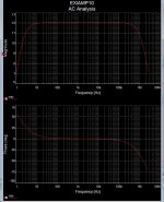
Here is a new and better version.
I have lowered supply to +/-16.0 Volt.
The Class A bias is 850mA.
The THD is 0.00007% at 1 Watt.
Max output at THD 0.100% is 9.7 Watt into 8 Ohm.

I have lowered supply to +/-16.0 Volt.
The Class A bias is 850mA.
The THD is 0.00007% at 1 Watt.
Max output at THD 0.100% is 9.7 Watt into 8 Ohm.
Of course you can. Download Kicad watch some tutorials and off you go.
Neither can I, but I am sure some other members have done pcb's for some of your other designs in the past.
But maybe you can express some rules for a layout - like witch components should go close etc...?
//
//
Ask prasi,he is a professional pcb designer. 😉I can't do it.
I need some help 🙂
Alex mm too.
Last edited:
prasi would have to do it as a GB or get paid somehow - his pcb designs are first class and this amp would be very simple and should have superb results with the active components as specified. The measurements that lineup have shown are first rate, so would be very interesting to see how the design sounds.
I have sent prasi a PM to see if he is interested.
I have sent prasi a PM to see if he is interested.
Last edited:
@ lineup - can I ask a couple of questions.
For your latest schematic as shown in post #6 - I assume pot R7 is to adjust Vout to be close as possible to 0VDC and pot R6 is to adjust the quiescent bias current in the output stage (850mA as you have shown)
For LED1 - is this any special type or colour?
For U4 and U5 - what should the Idss range be if selecting matched pairs - I have original Toshiba 2SK170BL's to select from.
Is hfe matching important for U1/U2 (2N5401)
Everything else is very clear and quite simple, very interested in hearing how this design sounds.
Regards,
Gary.

The polarity of the capacitors for the negative rail needs to be reversed.
Good eye, fixed.
I'm drawing some preliminary layouts, I'll let you guys know how it looks later.
We can probably leave out the 220u cap in feedback since we have a trimmer in the input stage
I'm drawing some preliminary layouts, I'll let you guys know how it looks later.
We can probably leave out the 220u cap in feedback since we have a trimmer in the input stage
Last edited:
Before you get to excited, challenge the amp with complex loads. 2 ohms, 100 ohms, with added inductance and capacitance. Not saying there will be a problem, but now is the time to find out. A zobel, or a zero in the miller compensation may be needed. Do a temp sweep on the output biasing as well.
- Home
- Amplifiers
- Solid State
- Scope Design: JFET Input EXICON Output 10 Watt Class A