You are right @Potentiallyincorrect, but implementing those changes in a layout will be pretty easy. But I do understand, that the schematic is far from finished.
I'm thinking 65x90mm layout to mount flat on the radiator. Should fit in a 2U chassis.
I'm thinking 65x90mm layout to mount flat on the radiator. Should fit in a 2U chassis.

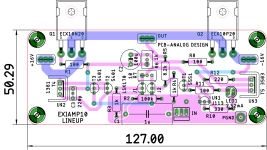


I assume PGND is the point to connect the negative terminal of the speaker output to? If that's the case you will want the GND terminal of R4 directly connected to this point and not via the PCB plane. Any currents induced there will negatively impact the NFB taken from this point. And yes, not only the speaker output gives negative feedback via R5 but also R4 does so.
PGND is the input / small signal gnd to be connected to PSU PCB ground. The output ground directly goes to PSU ground.
Then your GND terminal of R4 should also go directly to PSU ground. Reason as stated before. Any ever so small currents between PSU ground and the GND terminal of R4 will negatively impact NFB and thus THD performance. If you're aiming for THD < -120dB this WILL have an impact. I know this from building an actual amplifier with this kind of performance, not only from sims 😉
EDIT: you're probably better off connecting PSU GND to your pcb and put the speaker output terminal on it. And then branch off directly from the negative speaker output terminal to R4.
EDIT2: an example can be seen here: https://gitlab.com/t-5/amp-dr
The negative feedback for the inverting input of the diff amp is taken directly from the Speakon output connector via a net tie.
Last edited:
Nice work as usual prasi, you are so kind. Now, based on any mods with comments above on the ground terminals - i look forward to gerbers. I really want to see how this amp sounds based on lineup's measurements.
Thanks again for your great pcb designs around here.
Thanks again for your great pcb designs around here.
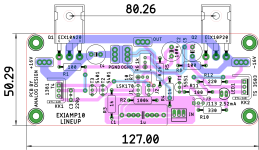
Also prasi, I would make the heavy GND connection(s) a faston terminal like you have for the +/- psu and speaker out.
I like lineup’s simulation design threads. They always bring some good discussion.
And, I confess, I am a sucker for any new-ish design with lateral mosfets. Bring it on, I say.
I hope some brave folks will build this and report on their findings.
And, I confess, I am a sucker for any new-ish design with lateral mosfets. Bring it on, I say.
I hope some brave folks will build this and report on their findings.
Yeh, I will order pcb's as soon as the gerbers appear here - hopefully thanks to prasi's great work.
I have all the components for this simple elegant design which measures well according to simulation by lineup.
I would also say Vunce will be having a go at it.
I have all the components for this simple elegant design which measures well according to simulation by lineup.
I would also say Vunce will be having a go at it.
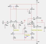
Have checked your schematic with lineup's - all seems fine.
One comment - you have shown the J113 fet as "U$1" on your schematic and the silk screen for the pcb, probably should be called J3.
Also, I would allow more holes for capacitor C1 to allow for different lead spacings for the input cap. Members like to use exotic caps here as well as more run of the mill film caps. You have done this on many other designs you have shown.
Apart from those comments and my one above in post #29 about ground connections, the pcb is a good size with good spacing for the output laterals.
Keep up the good work prasi.
Same here Gary, parts already in the bins. Probably can use the same chassis the “4Watter” was built in. 😉Yeh, I will order pcb's as soon as the gerbers appear here - hopefully thanks to prasi's great work.
I have all the components for this simple elegant design which measures well according to simulation by lineup.
I would also say Vunce will be having a go at it.

Well done again prasi, looks very good to me. Will get some pcb's ordered.
Looks interesting as always Lineup!
Anyone know where to find some ECX10 over here in Australia? Seems to be unavailable / unobtanium from the usual sellers.
Anyone know where to find some ECX10 over here in Australia? Seems to be unavailable / unobtanium from the usual sellers.
Anything under 100x100 is good because it qualifies for the $5 for 10 PCB rate at the usual fab houses 🙂You are right @Potentiallyincorrect, but implementing those changes in a layout will be pretty easy. But I do understand, that the schematic is far from finished.
I'm thinking 65x90mm layout to mount flat on the radiator. Should fit in a 2U chassis.
Thank you prasi!
You always support us! 🙏
PS. please, if you will find the time post the diy friendly single side pcb in pdf. 😉
You always support us! 🙏
PS. please, if you will find the time post the diy friendly single side pcb in pdf. 😉
Last edited:
I don't know any other supplier than Profusion electronic.Anything under 100x100 is good because it qualifies for the $5 for 10 PCB rate at the usual fab houses 🙂
https://www.profusionplc.com/parts/ecx10n20
- Home
- Amplifiers
- Solid State
- Scope Design: JFET Input EXICON Output 10 Watt Class A