Great build; I am going to point to something that you may choose to address...

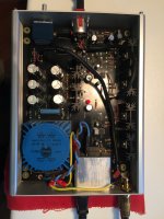
That proximity of mains wiring to PCB parts will be harmful and easily measurable if you start looking at let's say THD + N and then move that wiring away from the PCB. The parts affected are the optocoupler and its 2 caps... which is not the input, but the voltage-amplified input. Still, it may be noticeable by the ear if used by sensitive headphones. It will definitely show if you start measuring things... Consider bending the lugs a bit towards the transformer (away from those parts) and shorten the mains wiring length.
That proximity of mains wiring to PCB parts will be harmful and easily measurable if you start looking at let's say THD + N and then move that wiring away from the PCB. The parts affected are the optocoupler and its 2 caps... which is not the input, but the voltage-amplified input. Still, it may be noticeable by the ear if used by sensitive headphones. It will definitely show if you start measuring things... Consider bending the lugs a bit towards the transformer (away from those parts) and shorten the mains wiring length.
Thanks, I agree the AC wires could be shorter and the quick-connects bent a little to improve clearance.Great build; I am going to point to something that you may choose to address...
View attachment 1053408
That proximity of mains wiring to PCB parts will be harmful and easily measurable if you start looking at let's say THD + N and then move that wiring away from the PCB. The parts affected are the optocoupler and its 2 caps... which is not the input, but the voltage-amplified input. Still, it may be noticeable by the ear if used by sensitive headphones. It will definitely show if you start measuring things... Consider bending the lugs a bit towards the transformer (away from those parts) and shorten the mains wiring length.
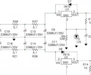
Well, heat is the enemy of electronics so I feel I must do something. Several options come to mind:-Be aware: By using only 1 primary, you have reduced the power of the transformer to 6,5VA. The reason that the voltage have dropped to 25VDC is that the transformer is being pushed extremely hard. the transformer can only deliver 0.13A and maximum half that continiusly if you want it to live.
- select and install a transformer with lower AC secondary voltage.
- Change the bias resistors from 60ma to 40ma
- Consider "improvements" to the PSU circuits such as ....
- Replace the 5.1 ohm resistors with higher wattage units
- Replace R37 and R38 with little boards having LM317, LM337 and 2 resistors each
What should I do about the stressed regulators?
Attachments

Thanks, I followed the guide and schematic. I tested the regulators with and without LEDs. I left it with green LEDs which tell me if power is upping correctly. Also I did not install the cover because I like the way it looks with all the tech showing.@fubar3, take a look at 6L6's build guide (first post here) for the section on LED reference configuration.
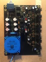
You're not supposed to stuff all resistors in that area if you're using LEDs:
View attachment 1053605
There are residuals voltages in the PCB because the big caps do not drain completely through the regulators. If power is removed when the HPs are unplugged, there is 130mv on the output which disappears when the HPs are plugged in again. This does no harm since there are not clicks or thumps when power is cycled.
Hi,
almost at the end of the building. In the guide I do not see a connection of pcb to the ground on the chassis: not necessary?
Tahnk you
Renato
almost at the end of the building. In the guide I do not see a connection of pcb to the ground on the chassis: not necessary?
Tahnk you
Renato
The guide advises to connect the pcb ground, which is near the volume control, to the common contacts of the input jacks, and then connect to the AC input switch assembly via a capacitor. Recent posts show this if you take a second look.Hi,
almost at the end of the building. In the guide I do not see a connection of pcb to the ground on the chassis: not necessary?
Tahnk you
Renato
Thank you! I realized in the guide what you suggest. Just wondering if a direct connection of the pcb to the star ground was also required.The guide advises to connect the pcb ground, which is near the volume control, to the common contacts of the input jacks, and then connect to the AC input switch assembly via a capacitor. Recent posts show this if you take a second look.
Hopefully this night (in Italy) my Whammy could work.
Thank you again
Renato
Only 1 gnd is required, according to the guide, through a capacitor. I made a direct wired connection to the Schurter tab, no capacitor.Thank you! I realized in the guide what you suggest. Just wondering if a direct connection of the pcb to the star ground was also required.
Hopefully this night (in Italy) my Whammy could work.
Thank you again
Renato
#4,517
I suppose this quick mod is plausible.... ?
Also, the voltage rails could stay at +18 and -18V for example for the output stage.. with the addition of a very low noise OP-AMP regulation (shunt?).... to allow for some nice (my all-time favourite + and - 12V max AD8066). OP's. Has anyone tried it (the additional regulation)? There's plenty of space inside the box.
Dear All,
finished my building, But unfortunately it does not work. I made first switch on using light bulb test and light bulb switched on. Indeed at pcb AC inlet I measure 175 VAC instead of 230VAC (I am in Europe). At C9 I measure 4.15V DC instead of 16 and between R13 and R14 0VDC instead of the expected 16. Obviously no sound at the headphone, juast a very light scratch when moving pot. The PSU test was OK before populating the rest of the pcb.
I attach a picture.
Very stupid error? Or can you address to a particular thread already discussing the steps required for diagnosis?
Thank you for your help
Renato
Attachments

I forgot to tell you the red leds switch on anywayDear All,
finished my building, But unfortunately it does not work. I made first switch on using light bulb test and light bulb switched on. Indeed at pcb AC inlet I measure 175 VAC instead of 230VAC (I am in Europe). At C9 I measure 4.15V DC instead of 16 and between R13 and R14 0VDC instead of the expected 16. Obviously no sound at the headphone, juast a very light scratch when moving pot. The PSU test was OK before populating the rest of the pcb.
I attach a picture.
Very stupid error? Or can you address to a particular thread already discussing the steps required for diagnosis?
Thank you for your help
Renato
renato
hmmmm... I do not have this amp (contemplating at the moment), but I had a look at your PCB and all seems okay... except the fact that you use 2 X 18V AC Talema... you see, with that bulb tester, the mains voltage drop might be large enough for voltage regs not to start regulating.... What is the DC voltage level at regs' IN pins??
Thanks, I agree the AC wires could be shorter and the quick-connects bent a little to improve clearance.
Rotate the IEC RF filter 180 deg.... as well.... 🙂
Of course, there might be a short somewhere that is causing a large current draw through the bulb.... I see that you used a custom case and decided to slide in the PCB... make sure the PCB tracks are not shorted to groundhmmmm... I do not have this amp (contemplating at the moment), but I had a look at your PCB and all seems okay... except the fact that you use 2 X 18V AC Talema... you see, with that bulb tester, the mains voltage drop might be large enough for voltage regs not to start regulating.... What is the DC voltage level at regs' IN pins??
I tested PSU before popul<ting the rest ofpcb: weverything was OK.hmmmm... I do not have this amp (contemplating at the moment), but I had a look at your PCB and all seems okay... except the fact that you use 2 X 18V AC Talema... you see, with that bulb tester, the mains voltage drop might be large enough for voltage regs not to start regulating.... What is the DC voltage level at regs' IN pins??
Renato
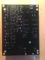
I removed the pcb from the chassis: still the same problem!I see that you used a custom case and decided to slide in the PCB... make sure the PCB tracks are not shorted to ground
renato
Hi,
I need your help, please!
Completed the Whammy kit but no sound. The light bulb tester switches on since at pcb AC input I measure 175 VAC instead of 230 VAC (I am in Europe). The red led (standard regulation) switches on, but at C9 pads 4.75 VDC instead of 15, whereas between R13 and R14 I measure 0VDC instead of 15.
The PSU test was ok before completing population of the rest of pcb. I replaced the op-amp without success and removed wiring to ground, input and output jacks, again no solution.
I also double checked resistors and caps.
I attach a couple of pictures of current populated pcb.
No idea on what to try next. Please help me or address me where I can find a diagnosis roadmap
Renato
Attachments
You need to take measurements to see where the current is flowing.
Try measuring the DC voltage across all four of the 10 ohm resistors (R16, R22, R29 and R32) that connect to the output FET's. There should be around 0.6 volts across each.
If the voltage across both the resistors is high then switch off and place a wire link across C13 and C23 and retest.
If the voltage across only one of the resistors in each channel is high then check for a short to ground at the output (the junction of the 10 ohm resistors)
Thankyou, I'll let you knowYou need to take measurements to see where the current is flowing.
Try measuring the DC voltage across all four of the 10 ohm resistors (R16, R22, R29 and R32) that connect to the output FET's. There should be around 0.6 volts across each.
If the voltage across both the resistors is high then switch off and place a wire link across C13 and C23 and retest.
If the voltage across only one of the resistors in each channel is high then check for a short to ground at the output (the junction of the 10 ohm resistors)
renTO
- Home
- Amplifiers
- Pass Labs
- "WHAMMY" Pass DIY headphone amp guide