

great work! STUNNING!schematics are public ... made some pcbs for me. Everything else is only diy. Dont want to share gerbers files, etc... If anyone is interested, I have permission from Papa to make a copy for myself UGS V6.
Made some modification, position of components. First is Muse attenuation, second is UGS module and last is buffer. SOUNDS GREAT. THX people...
🙂
have you been luck with getting the adapter boards?Including the other layer (in green) with GND, adapter looks like this.
Pins 2 and 4 of P4 "Encoder and LED I/F" connected to GND as well.
it seems this thread is near to death...
🙂
No, gionad not responding. I have done them myself and ordered yesterday.have you been luck with getting the adapter boards?
it seems this thread is near to death...
🙂
So sad that this thread is pretty much dead. I guess I am late with my build.
For JP5 you may use Samtec SSW-105-01-S-T +TSW-105-07-G-TAnyone has a p/n for JP5?
Are all caps 10nF and all resistors 10k?
Important: while looking back at Gionag's PCB (and yours), the debounce circuit as implemented seems weird (and to me eyes incorrect).
In case, I have redraw the way I would have implemented it myself.
Attachments
👍 very nice indeed.schematics are public ... made some pcbs for me. Everything else is only diy. Dont want to share gerbers files, etc... If anyone is interested, I have permission from Papa to make a copy for myself UGS V6.
Made some modification, position of components. First is Muse attenuation, second is UGS module and last is buffer. SOUNDS GREAT. THX people...
i don´t see the +3.3V connected to the adapter PCB...For JP5 you may use Samtec SSW-105-01-S-T +TSW-105-07-G-T
Important: while looking back at Gionag's PCB (and yours), the debounce circuit as implemented seems weird (and to me eyes incorrect).
In case, I have redraw the way I would have implemented it myself.
you have drawn pin9 (from P10 connector) as +3.3V but in schematic it is pin13 (see attached)
i am a bit confused...
🙂
Attachments
Alex wrote:
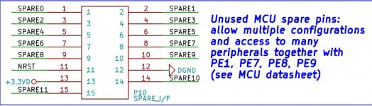
Stones, you are right for the GND pin location.
Gionag, you have the others pins PC6, PC7 and PC8 correctly marked on the spare I/F.
PC6 => SPARE5 (pin6)
PC7 => SPARE1 (pin2)
PC8 => SPARE0 (pin1)
GND (pin 12)
Spare connector pin numbering (from bottom view)
5 ..... 1
10 .... 6
15 ....11
so the correct pins of P10 would be PIN1, PIN2, PIN6, PIN12 and PIN13...
This is because I am using Samtec pin numbering convention which is different of the one used for the MCU controller.
13 .... 1
14 .... 2
15 .... 3
13 .... 1
14 .... 2
15 .... 3
Last edited:
Eric, thanks for those. I was prepared to use three single row pin header strips with the female counterparts.For JP5 you may use Samtec SSW-105-01-S-T +TSW-105-07-G-T
Ok, so we have
J2 pin3 - Ch_A2 - PC7 - P10 spareIF pin2
J2 pin5 - SW2_2 - PC8 - P10 spareIF pin1
J2 pin7 - Ch_B2 - PC6 - P10 spareIF pin6
GND - P10 spareIF pin12
+3.3V - P10 spareIF pin13
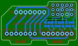
Here the dual encoder adapter board.
Use for
Mechanical encoder: C2,C3=10nF, R3,R4,R5,R6=10k
Optical encoder: R5,R6=0R, C2,C3,R3,R4=void
J2 pin3 - Ch_A2 - PC7 - P10 spareIF pin2
J2 pin5 - SW2_2 - PC8 - P10 spareIF pin1
J2 pin7 - Ch_B2 - PC6 - P10 spareIF pin6
GND - P10 spareIF pin12
+3.3V - P10 spareIF pin13
Here the dual encoder adapter board.
Use for
Mechanical encoder: C2,C3=10nF, R3,R4,R5,R6=10k
Optical encoder: R5,R6=0R, C2,C3,R3,R4=void
Attachments
Last edited:
Hi,schematics are public ... made some pcbs for me. Everything else is only diy. Dont want to share gerbers files, etc... If anyone is interested, I have permission from Papa to make a copy for myself UGS V6.
Made some modification, position of components. First is Muse attenuation, second is UGS module and last is buffer. SOUNDS GREAT. THX people...
are you sure about this ? :
First is Muse attenuation, second is UGS module and last is buffer. ? From what I can see from your video, you have: First Muse attenuation, second buffer, then the UGS module ?
Or, maybe you have done some modification, that I don't see ?
Last edited:
Hi,
are you sure about this ? :
First is Muse attenuation, second is UGS module and last is buffer. ? From what I can see from your video, you have: First Muse attenuation, second buffer, then the UGS module ?
Or, maybe you have done some modification, that I don't see ?
Yes, done some modification on pcbs.
This is not exactly copy-paste...there is coupling caps on board for V6 and this modification.
M1 socket is my gain stage...V6. Behind it is buffer...I can remove buffer and output is only gain stage.
Second option is, remove V6, remove buffer and and in place of the buffer I can put UGS V3.
Signal-flow is ok 🙂🤗
Second option is, remove V6, remove buffer and and in place of the buffer I can put UGS V3.
Signal-flow is ok 🙂🤗
O.K,
but do you have the right signal-flow in the circuit ? Is the gain stage before or after the Muses ?
Sounds OK to me now.Ok, so we have
J2 pin3 - Ch_A2 - PC7 - P10 spareIF pin2
J2 pin5 - SW2_2 - PC8 - P10 spareIF pin1
J2 pin7 - Ch_B2 - PC6 - P10 spareIF pin6
GND - P10 spareIF pin12
+3.3V - P10 spareIF pin13
Here the dual encoder adapter board.
Use for
Mechanical encoder: C2,C3=10nF, R3,R4,R5,R6=10k
Optical encoder: R5,R6=0R, C2,C3,R3,R4=void
I just noticed there is no thermal relief on the GND pin of P10.
Also check if there is enough clearance between the dual encoder adapter board and the Debug I/F (P1) - probably no issue if you placed a right angle header on P10.
Got inspired by PASS XP-32 characteristics?M1 socket is my gain stage...V6. Behind it is buffer...I can remove buffer and output is only gain stage.
Second option is, remove V6, remove buffer and and in place of the buffer I can put UGS V3.
Signal-flow is ok 🙂🤗
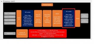
Me too. Here is my own implementation of a low output impedance UGS stage in an all_in_one module (shown here on my module test-bench).
In my case, I started from V4 but ended-up in a slight modified architecture to set the gain (using LTspice was quite helpful).
Besides the whammy style buffer, I also added a dc servo (output offset << 2mV)
All hand-soldered and getting old so be indulgent with my solders - one day I need to invest in a small reflow oven.
Got inspired by PASS XP-32 characteristics?
Me too. Here is my own implementation of a low output impedance UGS stage in an all_in_one module (shown here on my module test-bench).
In my case, I started from V4 but ended-up in a slight modified architecture to set the gain (using LTspice was quite helpful).
Besides the whammy style buffer, I also added a dc servo (output offset << 2mV)
All hand-soldered and getting old so be indulgent with my solders - one day I need to invest in a small reflow oven.
View attachment 1032851
looks very good...is it good, sound?
As I know in Pass XP-32 is ugs V7 with toshiba mosfets, point 8 in little 🙂
about this we can talk XP-12, XP-22...
we compared this version of mine wih pass X2.5. That "school" but v6 is better. 🙂
- Home
- Amplifiers
- Pass Labs
- UGS-muse preamp GB