Hello,
The result of my projects will never be free.
In the spirit of our passion, the amplifier pcb will be free of design costs.
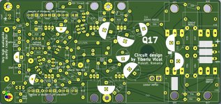
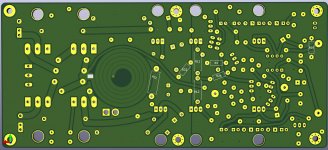
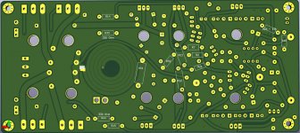
On 20-22-08-21 I will give the PCBs to the factory, a very small number of maximum 20 pieces, Q17 amplifier and Q17 power supply. After testing, I will open a buying group here on DiyAudio, in the special section. There will be multiple options: PCB, PCB + SMD, PCB + SMD + THD, but also finished modules, planted and tested.
I consider it beneficial for all colleagues to join a buying group because in this way everyone will benefit from very low prices, to the detriment of the personal development of the project!
Thanks for appreciation!
The result of my projects will never be free.
In the spirit of our passion, the amplifier pcb will be free of design costs.
On 20-22-08-21 I will give the PCBs to the factory, a very small number of maximum 20 pieces, Q17 amplifier and Q17 power supply. After testing, I will open a buying group here on DiyAudio, in the special section. There will be multiple options: PCB, PCB + SMD, PCB + SMD + THD, but also finished modules, planted and tested.
I consider it beneficial for all colleagues to join a buying group because in this way everyone will benefit from very low prices, to the detriment of the personal development of the project!
Thanks for appreciation!
As this is Tibi's initiative and thread, can you confirm that you do this in full cooperation with Tibi?
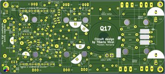
Q17 is an open source project. Anyone can design his own PCB, or use my design, to sell or make commercial amplifiers based on this design.
The project is now on github with a GPL3 licence that allow this.
I have no cooperation with Sorin, but he received my agreement to make his own PCB to make a commercial version.
Regards,
Tibi
The project is now on github with a GPL3 licence that allow this.
I have no cooperation with Sorin, but he received my agreement to make his own PCB to make a commercial version.
Regards,
Tibi
Last edited by a moderator:
There seem to be 4 options now for PCB's:
- Tibi's design (Gerber files);
- Tim's effort (Gerber files);
- Alex (no Gerber files yet);
- sorinsistem1 (good looking but apparently no Gerber files).
So, to make up a choice, you can imagine that I am a bit 😕😕😕😕
Let's put this way:
- my prototype design with embeded coil
- Tim's design that allow different parts and some extra flexibility
- Alex, so far the single 3 pair PCB, very well designed and I'm sure Alex will come with an even better one
- Sorin complete solution with protections and the stuff
I would like to see a better pcb that keep my embeded coil idea
Regards,
Tibi
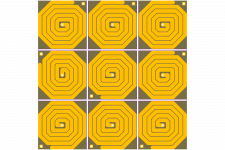
Did you measure (or calculate) the DC resistance of the embedded coil?
My rough calculation based on 35 mu thick copper traces gives some 0.2 ohm of DC resistance.
When I am right the coil is within the feedback loop (is it??) so maybe not an issue, but 0.2 ohm output resistance of any amplifier means a damping factor of 40 @ 8 ohm load.
My rough calculation based on 35 mu thick copper traces gives some 0.2 ohm of DC resistance.
When I am right the coil is within the feedback loop (is it??) so maybe not an issue, but 0.2 ohm output resistance of any amplifier means a damping factor of 40 @ 8 ohm load.
Last edited:
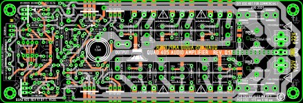
Hello,
I have ordered and set up the first boards in 35um copper. I brought the amplifier to its limit with +- 33V - that is when it starts to get messy with hearing protection. As a load I used 3-way speakers with very high quality drivers, which can be further tortured at a PA power amp. But it is also clear that I have reached the limit hereby, where the supply voltage was simply no longer sufficient, now this has nothing to do with the load of the transistors.
I do not find the 35um ideal and in the color green JLC-PCB 75um copper is "cheap". The second edition of the PCB I ordered in 75um and have already been delivered. However, I have not yet been able to assemble them. I am continuously working on the PCB layout.
What is not easy to solder in 75um are solid GND connections. Therefore I have changed that now. Also the backside assembly without printing is error sensitive, so I changed that as well.
The big Wima MKP10 are very important for me related to the small signal behavior of the amplifier, so this extra cost is ok for me. Large capacitors with more than 470uF I have not provided in my board layout, these must of course be present via short cables at the power connectors, that is out of question. Only from the geometry of the amplifier PCB it is important to me that the capacitors with > 1mF are located outside the board.
I have installed many 33nF FKP2, instead of the usual 100nF MKS. As it is a 5mm grid, this detail is up to everyone how precise capacitors - which quality - he wants to install.
For the footprints of the transistors and mosfet, the wide hole spacing now fits very well. All in all, soldering the large footprints is very comfortable for me. I have a 60W soldering station, for that it is optimal.
The use of my PCB layout requires a socketed OPA. I deliberately do without SMD components on the board. So it is much easier to solder for electronic amateurs like me.
Regards Tim
Attachments
Last edited:
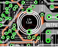
checked all the files and found that I did not put any pictures with PCB in inductor 🙂
The picture exists in the archive with the schematics, that I cannot attach at the moment.
The laminate will be 1.6mm, 2OZ (70u), ENIG gold finish.
Positioning is perpendicular to the PCB and soldering is done on both sides of the pcb, like an SMD component. The estimated DC resistance is 0.08R, the inductance is 1.2-1.3uH. It is clear that I will present these values when my PCBs come and make real measurements.
Attachments
Last edited:
Hello,
I consider it beneficial for all colleagues to join a buying group because in this way everyone will benefit from very low prices, to the detriment of the personal development of the project!
Thanks for appreciation!
I would be am interested in this group buy for sure, do you have a price/board in your mind? I would like to see some pics of the board layout,
Gabe
Did you measure (or calculate) the DC resistance of the embedded coil?
My rough calculation based on 35 mu thick copper traces gives some 0.2 ohm of DC resistance.
When I am right the coil is within the feedback loop (is it??) so maybe not an issue, but 0.2 ohm output resistance of any amplifier means a damping factor of 40 @ 8 ohm load.
In this morning I do not find my glasses ... I'm a bit blurry.
I used spiki to simulate and calculate inductance parameters. The measured dc resistance at 1oz=35 mu Cu is arounf 220mohm, very close to your calculation. In case you go for 2oz Cu this may be reduced to half.
It may be further reduced by redesigning the coil in 4 layer or by making the coil without solder mask and later cover with some Ag solder alloy.
Regards,
Tibi
PS. BTW, have you measured your speaker cables ?
Last edited by a moderator:
Hello Tim,
Your design brings to my memory the very first Germanium radios. 😀
Please do not put over the inductor large capacitors.
Regards,
tibi
Your design brings to my memory the very first Germanium radios. 😀
Please do not put over the inductor large capacitors.
Regards,
tibi
checked all the files and found that I did not put any pictures with PCB in inductor 🙂
The picture exists in the archive with the schematics, that I cannot attach at the moment.
The laminate will be 1.6mm, 2OZ (70u), ENIG gold finish.
Positioning is perpendicular to the PCB and soldering is done on both sides of the pcb, like an SMD component. The estimated DC resistance is 0.08R, the inductance is 1.2-1.3uH. It is clear that I will present these values when my PCBs come and make real measurements.
You may want to round (fillet) the tracks, so your coils will look bit smoother.
Regards,
Tibi
Hello Tim,
Your design brings to my memory the very first Germanium radios. 😀
Please do not put over the inductor large capacitors.
Regards,
tibi
Hello Tibi,
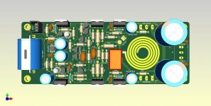
I have extended the PCB and it is now possible to solder very large electrolytic capacitors on it.
Regards Tim
Attachments
I used spiki to simulate and calculate inductance parameters. The measured dc resistance at 1oz=35 mu Cu is arounf 220mohm, very close to your calculation. In case you go for 2oz Cu this may be reduced to half.
It may be further reduced by redesigning the coil in 4 layer or by making the coil without solder mask and later cover with some Ag solder alloy.
Regards,
Tibi
PS. BTW, have you measured your speaker cables ?
Yes I did.
My power amps are next to my speakers; some 1 meter cable; DC resistance 0.004 ohm.
IMO, instead a PCB coil, it is preferable to use the normal copper wire air coil which will have negligible DC resistance (anyway that's what I will do 😉)
Hello,
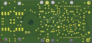
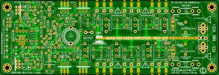
I have significantly changed the layout again, as I have found that soldering the transistors is not easy.
Therefore, I have now rotated the power transistors by 180°.
The board is now also completed with more labelling. It should be noted that Tibi has assigned the small MosFet differently in relation to the footprints in his KiCad model. Therefore, I have labelled the drain and source pins to help with installation.
The board is getting pretty good, I think. There is still room for further improvement, we'll see.
Regards Tim
Attachments
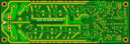
Revised board, with no ground plane . I hope will satisfied everyone .🙂
Regards,
Alex
Hi Alex, Your board looks impressive. My comments are,
-Input connection is correct? Doesn't match with the schematic.
-Coil footprint and power traces are overlapping.
-More gap between the fixings and nearby traces will be a good idea.
How do you wish to make your board available for us? Through a group buy?
Attachments
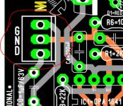


Hi Alex, Your board looks impressive. My comments are,
-Input connection is correct? Doesn't match with the schematic.
-Coil footprint and power traces are overlapping.
-More gap between the fixings and nearby traces will be a good idea.
How do you wish to make your board available for us? Through a group buy?
Input connector, are with two options, with and without, input capacitor, you can decide, which you want to use .
Coil footprint IMHO it's ok , coil can be mounted with insulated gap over PCB.
Nearby trace it's an ground trace and not will create problems . I ordered few PCB, and will test this amplifier . If it work well I'll post the gerbers right here .🙂
Regards, Alex
- Home
- Amplifiers
- Solid State
- Q17 - an audiophile approach to perfect sound