Have uploaded the project to GitHub - tvicol/Q17-a-QUAD405-audiophile-approach: Q17 is an error correction amplifier based on the QUAD405 current dumping principle
Regards,
Tibi
Regards,
Tibi
Hello,
I have a more interesting topic than the classification of the amplifier: component quality.
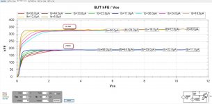
The reason is simple, I order MosFET here in Germany from Reichelt and the 2N7000 from Fairchild and the BS250 are not so satisfying. Two of the BS250s were already defective on delivery and one of the 2N7000s became unstable. So I bought Diodes ZVN4206A and ZVP2106A and compared them with my component tester.
I have attached the results in the zip folder, which are 24 pictures. I measured 2 pieces of each type completely. The rest I tested. I noticed that the MosFETs from Diodes have low variance and so far none have failed.
The ZVN4206A also behaves more linearly than the 2N7000.
So I would suggest these MosFET as an alternative for the amplifier.
Regards Tim
I have a more interesting topic than the classification of the amplifier: component quality.
The reason is simple, I order MosFET here in Germany from Reichelt and the 2N7000 from Fairchild and the BS250 are not so satisfying. Two of the BS250s were already defective on delivery and one of the 2N7000s became unstable. So I bought Diodes ZVN4206A and ZVP2106A and compared them with my component tester.
I have attached the results in the zip folder, which are 24 pictures. I measured 2 pieces of each type completely. The rest I tested. I noticed that the MosFETs from Diodes have low variance and so far none have failed.
The ZVN4206A also behaves more linearly than the 2N7000.
So I would suggest these MosFET as an alternative for the amplifier.
Regards Tim
Attachments
Nice work, Tim !
I'll give a try to ZVN4206A in a version with higher voltage rails. Seems to handle more Pd. Linearity as upper cascode transistor is not so critical as the lower one.
I'm using 2N7000-G from Microchip who is available from mouser and work just fine.
Regards,
Tibi
I'll give a try to ZVN4206A in a version with higher voltage rails. Seems to handle more Pd. Linearity as upper cascode transistor is not so critical as the lower one.
I'm using 2N7000-G from Microchip who is available from mouser and work just fine.
Regards,
Tibi
Last edited by a moderator:
Another idea:
The Q7 is a sound-sensitive component, so its quality is important for the result. The 2SC1845 is very well suited for this, as the transistors I received all deliver good measurement results (good = approximately linear amplification). A transistor that can do this even better, but has a much lower amplification factor, is the ZTX458. This transistor has no voltage problems because it is designed for 400V. If I understand the circuit correctly, the gain factor of Q7 is less critical, so this transistor is also an option, right?
https://www.mouser.de/ProductDetail/Diodes-Incorporated/ZTX458?qs=Ly%2FNF0nuwQ%252BDH7glPAJ3oQ%3D%3D
Attached is the comparison measurement:
Attachments
Q17 will operate at low Vce ~ 15V. You may use a low hfe transistor. Intentionally a large part of power dissipated by cascode is over top Q8 mosfet. There is no need for high Vce transistor. Any good old BC5XX will work just fine. Some BC5XX are very linear.
If you want to experiment, a npn Germanium will fit as well. Maybe AC181 or NTE101.
Overall, linearity of Q5 is more important than Q7.
Regards,
Tibi
If you want to experiment, a npn Germanium will fit as well. Maybe AC181 or NTE101.
Overall, linearity of Q5 is more important than Q7.
Regards,
Tibi
Last edited by a moderator:
Hi,
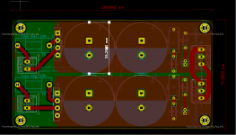
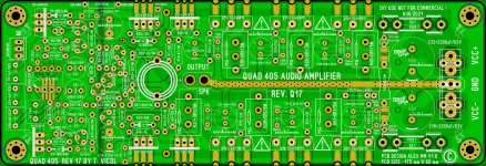
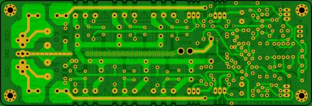
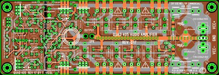
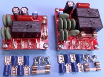
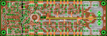
A small contribution to this project. PCB is not tested, maybe there are errors, maybe someone will check. If all goes well, I'll make the Gerber file available. I have always liked Quad and I made some copies. I'm posting some pictures.
A small contribution to this project. PCB is not tested, maybe there are errors, maybe someone will check. If all goes well, I'll make the Gerber file available. I have always liked Quad and I made some copies. I'm posting some pictures.
Attachments
Last edited:
Hi Alex,
I like that you have added castelated holes, decoupled each output mosfet with an electrolitic + foil and the option for smd and tht operational. On board fuses are always welcomed and some extra led's for rail indication are always good to have.
Power connector seems ... strong. Not sure what model is.
Thank you for taking your time to make a pcb for this design !
Very well done !
Regards,
Tibi
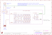
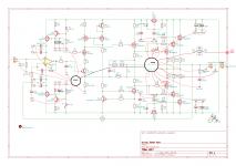
In the following we propose you to study our vision of practical realization of the amplifier QUAD405 (Q17).
Following the discussion with Mr. Tiberiu Vicol (author of the Q17 project) we decided to develop a printed circuit board (PCB) and some strictly necessary functional modules.
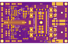
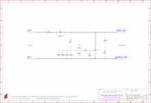
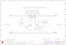
As a natural continuation I made a power supply module, at the same level of performance with the amplifier of Mr. Tiberiu Vicol.
From a functional point of view, the power source contains the following stages: rectification, filtering and a protection circuit based on a microcontroller.
This protection circuit monitors the AC voltage and performs delayed connection and instantaneous disconnection when it disappears to prevent unpleasant and destructive sounds in the audio enclosures(audio speakers).
Monitors the symmetrical supply voltage and in case of lack of one of the voltages or the appearance of an asymmetry, disconnects the acoustic enclosure.
It monitors the temperature by means of two precision thermistors placed on the radiators of the final floors. in case of a temperature higher than the threshold set at the initial calibration, in order to prevent damage to the final transistors, the acoustic enclosure will be disconnected.
When an overload of more than 10A (20A) occurs at the output of the amplifier, the acoustic enclosure will be disconnected. because the Q17 amplifier was designed without an SOA protection circuit (classic SOA protection circuits affect the sound reproduction of Current Damping amplifiers), we made a totally non-invasive protection circuit, which intervenes very precisely when acurrent through the acoustic enclosure, greater than 10A (20A), independently for each module amp`s.
All these protection states are displayed via a multicolored RGB LED.
The rectification / filtering stage contains some less known but particularly efficient technical solutions, among which we list: control of charging / discharging currents, CRC type cascade filtering and compensation of the output impedance in a wide frequency spectrum.
Due to the fact that the price of a high quality audio enclosure exceeds the price of an amplifier, we consider that their protection is essential.
To solve this problem, we consider it strictly necessary to mount an additional Crowbar protection circuit combined with an amplifier protection circuit against capacitive loads that can damage the final floor under certain conditions.
for a complete list of all functional modules of a high quality amplifier, it is strictly necessary the presence of modules: DC-Trap, Lift GROUND and SOFT-START. the DC-Trap module has the role of separating the continuous (unwanted) component superimposed accidentally and randomly over the AC voltage, applied to the terminals of the primary winding of the mains transformer; The GROUND Lift module has the role of raising the potential of the audio mass relative to the terminalearthing of the chassis and metal parts connected to the protection pin of the IEC type network connector; The SOFT-START module has the role of limiting the initial current (Inrush Current) at start-up due to the saturation of the magnetic core of the toroidal transformer and electrolytic capacitorsfrom the filtration floor. For total compatibility we recommend the use of DC-Trap-01 and DC-Trap-02 modules which also have the GROUND Lift circuit in the component and the SS-01 and SS-02 SOFT-START modules which are part of the offer of products dedicated to high performance DIY constructions.
If you want a buying group for these PCBs, kits or modules planted and tested, please guide me in this regard, I have no experience on this site.
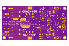
In Romania, we launched this project on a FB group dedicated to Romanians. On 05/08/21 I give the first PCBs to the factory.
To view all the files on the Q17-AMP project, please download and view all the files in the attached archive.
Thank you!
Following the discussion with Mr. Tiberiu Vicol (author of the Q17 project) we decided to develop a printed circuit board (PCB) and some strictly necessary functional modules.
As a natural continuation I made a power supply module, at the same level of performance with the amplifier of Mr. Tiberiu Vicol.
From a functional point of view, the power source contains the following stages: rectification, filtering and a protection circuit based on a microcontroller.
This protection circuit monitors the AC voltage and performs delayed connection and instantaneous disconnection when it disappears to prevent unpleasant and destructive sounds in the audio enclosures(audio speakers).
Monitors the symmetrical supply voltage and in case of lack of one of the voltages or the appearance of an asymmetry, disconnects the acoustic enclosure.
It monitors the temperature by means of two precision thermistors placed on the radiators of the final floors. in case of a temperature higher than the threshold set at the initial calibration, in order to prevent damage to the final transistors, the acoustic enclosure will be disconnected.
When an overload of more than 10A (20A) occurs at the output of the amplifier, the acoustic enclosure will be disconnected. because the Q17 amplifier was designed without an SOA protection circuit (classic SOA protection circuits affect the sound reproduction of Current Damping amplifiers), we made a totally non-invasive protection circuit, which intervenes very precisely when acurrent through the acoustic enclosure, greater than 10A (20A), independently for each module amp`s.
All these protection states are displayed via a multicolored RGB LED.
The rectification / filtering stage contains some less known but particularly efficient technical solutions, among which we list: control of charging / discharging currents, CRC type cascade filtering and compensation of the output impedance in a wide frequency spectrum.
Due to the fact that the price of a high quality audio enclosure exceeds the price of an amplifier, we consider that their protection is essential.
To solve this problem, we consider it strictly necessary to mount an additional Crowbar protection circuit combined with an amplifier protection circuit against capacitive loads that can damage the final floor under certain conditions.
for a complete list of all functional modules of a high quality amplifier, it is strictly necessary the presence of modules: DC-Trap, Lift GROUND and SOFT-START. the DC-Trap module has the role of separating the continuous (unwanted) component superimposed accidentally and randomly over the AC voltage, applied to the terminals of the primary winding of the mains transformer; The GROUND Lift module has the role of raising the potential of the audio mass relative to the terminalearthing of the chassis and metal parts connected to the protection pin of the IEC type network connector; The SOFT-START module has the role of limiting the initial current (Inrush Current) at start-up due to the saturation of the magnetic core of the toroidal transformer and electrolytic capacitorsfrom the filtration floor. For total compatibility we recommend the use of DC-Trap-01 and DC-Trap-02 modules which also have the GROUND Lift circuit in the component and the SS-01 and SS-02 SOFT-START modules which are part of the offer of products dedicated to high performance DIY constructions.
If you want a buying group for these PCBs, kits or modules planted and tested, please guide me in this regard, I have no experience on this site.
In Romania, we launched this project on a FB group dedicated to Romanians. On 05/08/21 I give the first PCBs to the factory.
To view all the files on the Q17-AMP project, please download and view all the files in the attached archive.
Thank you!
Attachments
-
 Q17-SUPPLY-SCH.png120.5 KB · Views: 674
 -
 Q17-SUPPLY-TOP - Copy.png553.8 KB · Views: 529
 -
 Q17-SUPPLY2.png191 KB · Views: 444
 -
 Q17-SUPPLY.png220.3 KB · Views: 439
 -
 Q17-AMP-COOL2.png136.7 KB · Views: 468
 -
 Q17-AMP-COOL.png163 KB · Views: 496
 -
 Q17-AMP-TOP.png45.5 KB · Views: 491
 -
 Q17-AMP-BOTTOM.png27.9 KB · Views: 528
 -
 Q17-AMP-ALL-HI.png350 KB · Views: 598
 -
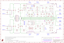
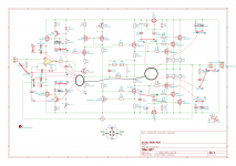
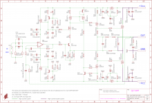 Q17-AMP-SCH.png119.4 KB · Views: 673
Q17-AMP Audio Accesories!
Attachments
-
 Q17-OTP-SCH.png54.3 KB · Views: 445
 -
 SAMPLE-1.jpg90.3 KB · Views: 378
 -
 SS-Both-1.jpg139.8 KB · Views: 426
 -
 SS-02-2.jpg142.7 KB · Views: 402
 -
 Q17-OTP-ALL.png73.7 KB · Views: 363
 -
 Q17-OTP-TOP.png10.7 KB · Views: 409
 -
 DC-Trap-02-SCH.png85.6 KB · Views: 448
 -
 DC-Trap-Both-1.jpg129.9 KB · Views: 430
 -
 DC-Trap-2-3.jpg95.3 KB · Views: 464
 -
 SS-02-SCH.png70.9 KB · Views: 542
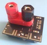
Thanks for the appreciation, I specify that that DC power connector, is with screw, or fast on to choose.
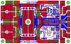
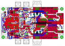
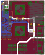
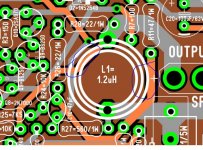
I made a mistake, passing routes under the coil, that is part of that bridge, I corrected, and after a thorough check, I will post the corrected PCB.
If there, are other observations, changes to be made, please let me know. I'm glad to be of help with my little skill. 🙂
Regards
Alex
I made a mistake, passing routes under the coil, that is part of that bridge, I corrected, and after a thorough check, I will post the corrected PCB.
If there, are other observations, changes to be made, please let me know. I'm glad to be of help with my little skill. 🙂
Regards
Alex
Attachments
Alex
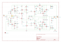
Unfortunately your PCB version has some major routing issues... The GND connection from the source to the amplifier should never carry current, it should ONLY be for decoupling the power supply(GND). If you want the output minus terminal to be connected to the amplifier module, then you will have to pull another GND connection(GND-P), otherwise through the R32 resistor, which is not at all correctly placed in terms of GND routing, you will pollute the entire input GND(GND-A) with noise ... R32 is just a routing compromise so that there is no longer a second(GND) or third GND(GND-P) connection between the power supply board and the amplifier board ...
The R32 must be connected as close as possible to the GND-Power terminal.
The connection of the GND(minus) terminal of the acoustic enclosure must be made from the power supply board, otherwise they will dirty the GND layer of the amplifier module.
Basically Tibi made about the same mistake in the demonstration amplifier...
GND-A: GND Input
GND: GND for Amp Module, ONLY for decoupling
GND-P: GND Power, for Output Terminal, Acoustic Enclosure
Thank you!

Hi Alex,
Nice pcb design. Pls see my minor comments.
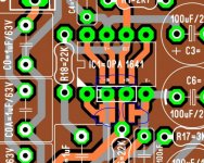
-what are the left over traces around the op-amp pins for? Are they for EMI protection?
-partial pcb traces are still visible within the coil footprint.
-R32 is a ground loop breaker. one end should go to the chassis, the other to the power supply ground. You could omit this from your pcb design as it could be implemented as a standalone connection between the chassis and the psu ground.
Excellent pcb design, thanks.
Nice pcb design. Pls see my minor comments.
-what are the left over traces around the op-amp pins for? Are they for EMI protection?
-partial pcb traces are still visible within the coil footprint.
-R32 is a ground loop breaker. one end should go to the chassis, the other to the power supply ground. You could omit this from your pcb design as it could be implemented as a standalone connection between the chassis and the psu ground.
Excellent pcb design, thanks.
Attachments
Hi Alex,
Pls see attached sketches.
Each black circle is a ground plane or star ground
First circle/star is for the op-amp/vas section.
The second circle/star is for the power section.
Both circles/planes/stars are connected to each other.
The house ground is connected to the chassis with the loop breaker.
This amp deserves more attention.
Attachments
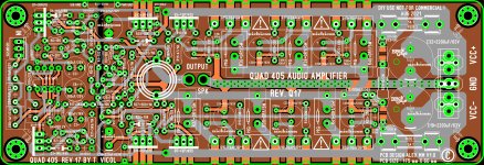
Sorry for the omission!
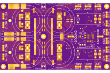
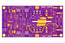
Q17-AMP
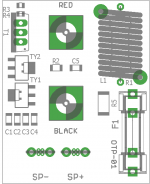
PCB-AMP: 115x60mm, FR4, 1oz, Black or Blue.
PCB-Coil (coil): 38x38mm, FR4, 2oz, Gold finished, no colors.
Q17-SUPPLY
PCB-SUPPLY: 127x78mm, FR4, 1oz, Black or Blue.
All selected components are audiophile and rated HIGH-END: VISHAY resistors, Nichicon capacitors, Wima, Arcotronics, Epcos. Brand Name only transistors, original, from the most reliable sources, TME, Mouser.
Q17-AMP
PCB-AMP: 115x60mm, FR4, 1oz, Black or Blue.
PCB-Coil (coil): 38x38mm, FR4, 2oz, Gold finished, no colors.
Q17-SUPPLY
PCB-SUPPLY: 127x78mm, FR4, 1oz, Black or Blue.
All selected components are audiophile and rated HIGH-END: VISHAY resistors, Nichicon capacitors, Wima, Arcotronics, Epcos. Brand Name only transistors, original, from the most reliable sources, TME, Mouser.
Hi Alex,
Expanded the grounding scheme to include your additional power MOSFETs decoupling caps.
Separated the take offs for the speaker return and PSU return.
Completed the ground lift connection.
It would be a good idea to add one or two spare parallel GND connectors (0V) on the PSU connection header traces.
Attachments
PCB Tombola...
There seem to be 4 options now for PCB's:
- Tibi's design (Gerber files);
- Tim's effort (Gerber files);
- Alex (no Gerber files yet);
- sorinsistem1 (good looking but apparently no Gerber files).
So, to make up a choice, you can imagine that I am a bit 😕😕😕😕
There seem to be 4 options now for PCB's:
- Tibi's design (Gerber files);
- Tim's effort (Gerber files);
- Alex (no Gerber files yet);
- sorinsistem1 (good looking but apparently no Gerber files).
So, to make up a choice, you can imagine that I am a bit 😕😕😕😕
- Home
- Amplifiers
- Solid State
- Q17 - an audiophile approach to perfect sound