Another option for those who have already built the D3 and want to reduce R21 to 4K7 is to piggyback a 62K resistor on top. I find desoldering SMD parts much more difficult than soldering them. So I'm going for the additive solution!
Good option!

Although, there is an easy way to desolder. Just put enough solder on your tip to touch both sides of the resistor at the same time, comes right off in a second.

Many thanks to my local friend @har297 (Harsha) in helping to solder all the SMD parts of my D3 and I2S simultaneous boards I could make my dream of TDA dac come true 🙂 Using the Pedja IV stage boards and now my best dac ever built. Using all my Salas clone psu boards along with one diyinhk LT3042 for 5v/3.3v its playing some of the best music in my setup of USSPA + J2 mono blocs.


Thank you Ryan for the excellent dac board and design.
Thank you Ryan for the excellent dac board and design.
Last edited:
Thank you Ryan for the excellent dac board and design.
Hi manniraj,
You're very welcome. Very neat build, well done!
Good option!
Although, there is an easy way to desolder. Just put enough solder on your tip to touch both sides of the resistor at the same time, comes right off in a second.
Using a wide solder tip so you can touch both ends of the component at the same time is an easy solution for desoldering small smd parts.
Hi,
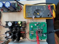
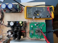
I have a problem with my D3 board. It has been running nicely for a few weeks but today it malfunctioned. I checked the power supply lines and there seems to be a problem with the voltages.
On the TDA chip I read the following voltages:
Pin 15 (-15v)=+5v
Pin 26 (-5v)=+15,1v
Pin 28 (+5v)=25,1v
V1 input =26,75v
V1 output= 25,11v
CC1 input=5,1v
CC1 output=1,24v
Can anybody tell me which component is defective?
I am afraid the TDA chip did not survive...
Hi,
I have a problem with my D3 board. It has been running nicely for a few weeks but today it malfunctioned. I checked the power supply lines and there seems to be a problem with the voltages.
On the TDA chip I read the following voltages:
Pin 15 (-15v)=+5v
Pin 26 (-5v)=+15,1v
Pin 28 (+5v)=25,1v
V1 input =26,75v
V1 output= 25,11v
CC1 input=5,1v
CC1 output=1,24v
Can anybody tell me which component is defective?
I am afraid the TDA chip did not survive...
Hi Supersurfer,
Did you by any chance ground the negative on the 26V supply at any point? Those voltages seem to indicate this scenario. If you did you would have had 15W across V1(according to LTspice) which may not have survived.
Last edited:
Hi,
I have a problem with my D3 board. It has been running nicely for a few weeks but today it malfunctioned. I checked the power supply lines and there seems to be a problem with the voltages.
On the TDA chip I read the following voltages:
Pin 15 (-15v)=+5v
Pin 26 (-5v)=+15,1v
Pin 28 (+5v)=25,1v
V1 input =26,75v
V1 output= 25,11v
CC1 input=5,1v
CC1 output=1,24v
Can anybody tell me which component is defective?
I am afraid the TDA chip did not survive...
Oh no... were you running your S1 chip?
Hope not,
Aguaazul
Supersurfer,
Just thinking about this some more. Is your D3 ground floating? Are these voltages taken with reference to D3 ground? I ask because it looks like the shunt regs are still regulating the 10V difference (-5 to -15 and -5 to +5) that they should. If this is the case your 1541 ground will be floating at 20V. Do you have your digital inputs galvanically isolated? And your output stage?
Where did you have your ground lead connected when taking these voltages?
I think these voltages are close to what I have If I would reference the ground lead to the negative of the -26V supply. The only difference is in changing R21 from 5k1 to 4k7 gives higher voltage drop across V1 and less across CC1.
Have you changed R21 to 4k7? Doesn't look like you have.
Last edited:
Hi Ryanj,
I see I made a mistake of measuring referenced to -26v pin I measured again, see attached pictures.
Pin 15=-16,17v
Pin 26=-6,17v
Pin 28=7,24v
The input voltage from the Salas regulator is 27,05v
There was no output stage, only iv resistor, input from your i2s-pcm board.
Power supplies are all isolated. (Also separate transformer windings)
Is there a defective ps component in your view? How can the voltages be adjusted to be within dac limits?
I see I made a mistake of measuring referenced to -26v pin
I measured again, see attached pictures.Pin 15=-16,17v
Pin 26=-6,17v
Pin 28=7,24v
The input voltage from the Salas regulator is 27,05v
There was no output stage, only iv resistor, input from your i2s-pcm board.
Power supplies are all isolated. (Also separate transformer windings)
Is there a defective ps component in your view? How can the voltages be adjusted to be within dac limits?
Attachments

Supersurfer
Out of curiosity, can you confirm that when you initially built the board these same measurements were -15,-5,+5v?
Also, wouldn't the shift in these voltages all result if the LM317 is now out of spec? I'd measure the value across R16,17&21 to see if they are still in spec. Could be a bad solder joint starting to degrade?
Last edited:
The +5V and -5V final regulation circuits look suspect. Perhaps X1 and X2 (TL431) are faulty. That can be checked by measuring the voltage drop across R20 and R25. They should measure 2.5V (Vref for TL431) if the TL431 are working.
The TL431 in SMD package are easily damaged by too much heat during soldering. I know from personal experience. 🙂
The TL431 in SMD package are easily damaged by too much heat during soldering. I know from personal experience. 🙂
The measurements were within spec when I finished the board so something has changed.
@Ben Mah:
I will check the tl431 smd’s by measuring the voltages. Thanks for the suggestion!
Today I changed r21 value to 4,7k, this does not change the voltages.
@Ben Mah:
I will check the tl431 smd’s by measuring the voltages. Thanks for the suggestion!
Today I changed r21 value to 4,7k, this does not change the voltages.
Supersurfer,
Im leaning towards solder joint issues on X1 and X2. X3 looks like its working.
First thing I would do is use some flux and reflow the pins on X1 and X2 and all the resistors connected.
Im leaning towards solder joint issues on X1 and X2. X3 looks like its working.
First thing I would do is use some flux and reflow the pins on X1 and X2 and all the resistors connected.
Last edited:
Supersurfer,
Im leaning towards solder joint issues on X1 and X2. X3 looks like its working.
First thing I would do is use some flux and reflow the pins on X1 and X2 and all the resistors connected.
Yes that has done it! I think bad solderings got loose due to heat during operation. I resoldered x1 and x2 and all voltages are correct again.
Thanks for the suggestion Ryanj!
These tl431 are the most tedious components to solder, the pads are very small and you risk burning the part with soldering, like Greg noted in his tutorial: order a bunch of spares!
Next up is to test if the chip is stil functioning, with a bit of luck the voltages did not pass the absolute maximum voltages according to the datasheet: 7 and 17v.
If defective I need to ask Aquaazul to return me a S1 chip 😛
Glad to hear that, let's hope that your s1 chip survived the abuse. Only .24V past the max... Might be ok.
The TDA chip is OK, everything is working again!
Aguaazul can relax😀
I ordered a pair of Sowter 1465 IV transformers as a result of your experiences. Will be delivered in a week or so.
Aguaazul can relax😀
I ordered a pair of Sowter 1465 IV transformers as a result of your experiences. Will be delivered in a week or so.
- Home
- Group Buys
- DIY TDA1541A PCB "D3"