There are a number of hall current sensors in the market. I looked at options since current probes are expensive and mostly aimed at high current. Below is what I found. The Honeywell looked the best for this application. It also suggests winding a number of turns through your existing probe too increase its sensitivity is an option. Put the probe on the ground side of the transformer.
I think something like this ACS37002: 400 kHz, High Accuracy Current Sensor could be quickly turned into a useable isolated current probe. It claims 10KV isolation.
Something like this is an alternate option https://www.lem.com/sites/default/files/products_datasheets/cd 100 s sp8 f.pdf
Or this: Pololu - ACHS-7121 Current Sensor Carrier -10A to +10A
Or this https://sensing.honeywell.com/honeywell-sensing-cslw-series-product-sheet-005861-1-en.pdf in stock at Digikey for $17 Blocked Its an odd one and you would need to calibrate its response curve but it may be a solution.
Not really, it's easy once you've figured out how to equalize the probe. I could even use a series resistor of say 6Meg directly into a 600R input of the AP.
@Hans: I have measured on one transformer but with the other one loaded with an identical 1M/1k divider.
Jan
@Hans: I have measured on one transformer but with the other one loaded with an identical 1M/1k divider.
Jan
Building a differential HV probe is not simple but not too difficult and could be rewarding.
First- at high voltages resistors are not necessarily resistors. You would need several in series and they should be resistors with a low voltage coefficient. (Same for the HV amp feedback network.) Then you need to compensate for the input C of the cable and AP/Whatever its connected to. On a low voltage probe a cap in parallel with the resistors works but at high voltage not so easy. The big Tek probes (P6015) have a cylinder around the resistor that is tapered to make the shunt cap. I think you could do this with some clever PCB layout. Finally you would need some trimmer resistors to adjust the attenuation and trim caps to optimize the CMRR vs. frequency. Lots of good execution details here: Basics of High Voltage Probe Design
First- at high voltages resistors are not necessarily resistors. You would need several in series and they should be resistors with a low voltage coefficient. (Same for the HV amp feedback network.) Then you need to compensate for the input C of the cable and AP/Whatever its connected to. On a low voltage probe a cap in parallel with the resistors works but at high voltage not so easy. The big Tek probes (P6015) have a cylinder around the resistor that is tapered to make the shunt cap. I think you could do this with some clever PCB layout. Finally you would need some trimmer resistors to adjust the attenuation and trim caps to optimize the CMRR vs. frequency. Lots of good execution details here: Basics of High Voltage Probe Design
Attachments
Jan-One other aspect that's important to check. You calibrated the probes with a low impedance source for all intents and purposes. You should check the response of the probes with a 1 Meg resistor in series with the probe to make sure there are no unintended impedance related errors. The impedance at the output of the transformer is not that low and the probe could interact so its worth checking.
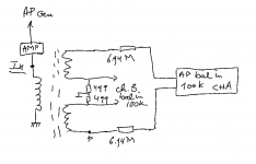
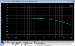
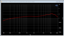
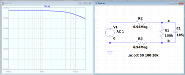
Alright, did some more measurements today. Constructed a high impedance probe (~14Meg across both transformer outputs) and looked at the probe response. The two 6.94Meg resistor are high-voltage 7.5kV rated resistors. Based on earlier posts, I assume that this impedance does not appreciably impact the secondary output voltage.
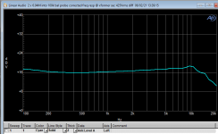
Then I used the probe response to eq the measurement of the freq response at the secondary output. Vo at the secondaries was about 400Vrms (the absolute value of the Y-axis can be disregarded).
The conclusion I draw from this is, that when I drive my direct drive amp with a flat response, the output should be equalized as in the 3rd graph.
Jan
Attachments
Last edited:
The next attachment is the panel current as measured with 2 x 499R in the panel ground leads as shown in the previous post. This measurement does not need a probe eq but I used regulation on the input to the speaker of 3V +/-2%, which gave about 400Vrms at the secondaries at 1kHz.
The peak current is about 2.2mA at around 10kHz. For my target of 1500Vrms full output, that would mean a peak current requirement of about 8mA at 10kHz.
Jan
The peak current is about 2.2mA at around 10kHz. For my target of 1500Vrms full output, that would mean a peak current requirement of about 8mA at 10kHz.
Jan
Attachments
Last edited:
Jan,
It’s not clear to me how you got from the second to the third image in #345.
I would expect the curve in the third image to go up instead of down at 20Khz and also the shape of the third curve does not seem to correlate with the second curve ?
Hans
It’s not clear to me how you got from the second to the third image in #345.
I would expect the curve in the third image to go up instead of down at 20Khz and also the shape of the third curve does not seem to correlate with the second curve ?
Hans
Add 2 extra bass panels (989 config) and get more bass and a more even current load!
Yes, I might still do that, I have some spare panels.
But first get the direct drive amp done!
Jan
Jan,
It’s not clear to me how you got from the second to the third image in #345.
I would expect the curve in the third image to go up instead of down at 20Khz and also the shape of the third curve does not seem to correlate with the second curve ?
Hans
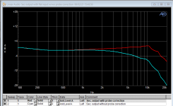
Hans, the 2nd graph shows the drooping response of the voltage probe shown in the first drawing. It is mainly due to the input capacitance of the AP across the 100k Rin. The flat one is a 'loop back' corrected with the inverted probe response, leading to a flat response as expected.
This corrected probe response is then used to equalize the input voltage, and measure the output voltage. Without the correction, the output voltage would droop very much due to the droop of the 'probe'. The correction EQ raises the input voltage according to the inverse of the drooping probe response to compensate for it so that the measurement can be considered flat.
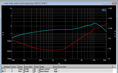
There is no correlation between the 2nd and the 3rd graph, as such. But here is a comparison of the xformer output with and without the probe correction. This compares with the 3rd graph in # 345.
Jan
Attachments
Last edited:
Are your numbers rms or peak? And you should look at the phase relationship between volt and current to see what the devices need to handle.
It's all RMS, and yes, good point. So far I have assumed that the load is predominantly capacitive but that may not be the case.
Jan
Jan
The conclusion I draw from this is, that when I drive my direct drive amp with a flat response, the output should be equalized as in the 3rd graph.
How then is the third graph made when it is not correlated to the voltage correction curve ?
It seems that you assume that the only reason for a FR droop of your probe is the input capacity of the AP, however in the simulations it can be seen that the secondary voltage is not at all flat.
So I’m a bit lost.
Hans
Hans, my reasoning is as follows. If the probe has a flat response, and I feed the speaker with a flat response, then what I measure with the probe gives me the response from speaker input to the panels (output of secondary). This is not a flat response, and my direct drive amp should mimic this response; the dd amp sort of 'replaces' the xformer.
However, my probe is not flat but falls with frequency.* So to correct for the falling probe response, I normalize the probe response to 0dB at 100Hz, and then apply the inverse of this response to the speaker input level, so my measurement will 'look like' I measured with a flat probe.
So maybe a semantic issue or my misunderstanding, that there is of course a connection between the 2nd and 3rd graph, not sure what 'correlation' between them would mean.
Jan
*I suspect this is due to AP input cap but really the cause is not of importance for the measurement.
Jan. It looks like the peak voltage is at 90 degrees. That suggests the output devices will have the full supply voltage across them at peak current at around 10 KHz. Need good heat sinks.
I would not worry about response at this phase. Equalize the system as a system.
I would not worry about response at this phase. Equalize the system as a system.
Yes, so at and above 10k, the load is pretty much capacitive. I have been working with that assumption, and my device dissipation remains within limits, even without the low duty cycle of high frequency signal components.
Jan
Jan
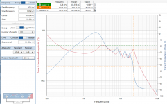
Finally, an impedance measurement with the Bode100 in series-thru mode. Measured between the two wires going from the xformers to the panels, disconnected from the xformer.
Lots of funny things seem to be going on in the upper octave!
Jan
Lots of funny things seem to be going on in the upper octave!
Jan
Attachments
- Home
- Loudspeakers
- Planars & Exotics
- QUAD 63 (and later) Delay Line Inductors