Are the CAL knobs in the correct position? If I remember well, you have to turn them all the way to the left until you feel that there is a switch switching, otherwise you get the right waveform, but at arbitrary scales.
There are also a couple of things in the circuit that could cause an oscillation at a too high frequency, but I have to start up a computer and serve a cat before I can get back to you about those.
There are also a couple of things in the circuit that could cause an oscillation at a too high frequency, but I have to start up a computer and serve a cat before I can get back to you about those.
Right you are. Just pushed the hor cal knob all the way right till it clicked and 27MHz is the answer. Vertical call knob was correctly positioned.
What does the signal at R124 look like when you measure DC coupled with a 1:10 probe? How is the waveform positioned with respect to 0 V?
Does R124 make contact with J5 pin 47?
Edit: I just checked my own Verilog code and the voltage across R129 can't have anything to do with it.
Does R124 make contact with J5 pin 47?
Edit: I just checked my own Verilog code and the voltage across R129 can't have anything to do with it.
Last edited:
Do you see any signal at R95 or R96 with respect to ground? A 13.5 MHz square wave, for example, or a rather irregular signal?
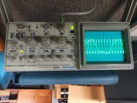
See attached waverform with 1:10 probe but AC coupled (could get no sweep when DC coupled - was not triggering). Looks like 4Vpp. Also looks more 'square'. Am not sure what is happening with the x1 probe showing circa 1Vpp and the x10 probe 4Vpp...is it simply resolution?
Not sure exactly what you mean "waveform positioned with respect to 0V, but I measured the same locations as the scope probes (between R124 and R52 and got 265Vdc.
R129 with 85A3 ignited is 3.328Vdc drop.
R125 makes contact with J5.47 pad, but the pin contact is sketchy. I'll reflow it now.
Not sure exactly what you mean "waveform positioned with respect to 0V, but I measured the same locations as the scope probes (between R124 and R52 and got 265Vdc.
R129 with 85A3 ignited is 3.328Vdc drop.
R125 makes contact with J5.47 pad, but the pin contact is sketchy. I'll reflow it now.
Attachments
I was wondering why the clock signal was so small, it can't be due to the scope with a 50 MHz scope bandwidth. It's probably the big capacitive load from the 1:1 probe that caused it. The signal you get with a 1:10 probe looks fine. By the way, R52 is at -300 V rather than ground.
All in all, you have a good looking clock signal at R124 and the ignited85A2 signal (voltage across R129) is also fine. I'm curious to read what will happen when you have resoldered J5 pin 47.
All in all, you have a good looking clock signal at R124 and the ignited85A2 signal (voltage across R129) is also fine. I'm curious to read what will happen when you have resoldered J5 pin 47.
Still no sound via JLSounds I2S.
Filter switch still not functioning properly. Not sure what is causing that problem. Positions 1, 2, 3 all working as intended, position 4 grounded regardless of the switch position (never sees 3.3V when not activated). No sound from relays.
Filter switch still not functioning properly. Not sure what is causing that problem. Positions 1, 2, 3 all working as intended, position 4 grounded regardless of the switch position (never sees 3.3V when not activated). No sound from relays.
When you connect a 1:10 probe between a pad of R95 and ground or between a pad of R96 and ground (so not -300 V), what do you see?
What's the collector-emitter voltage of Q15 and what's the voltage across R134?
What's the collector-emitter voltage of Q15 and what's the voltage across R134?
Last edited:
So you have a good-looking clock signal at R124, checked and resoldered the clock connection to the FPGA module and still the FPGA refuses to make net "relay" high or to release the reset of the sigma-delta modulator, which it should normally do a few seconds after detecting a good 27 MHz clock... I have to think about this one.
Would not be surprised if it is still a FPGA solder issue. Will have dinner and then check the inside of J5 for continuities. Another FPGA removal...yikes.
I hope that's it, because I haven't found anything else that could cause it, except maybe a completely wrong value for R124.
Just spent a few hours continuity checking all 160 pins on the FGPA sockets and have found nothing. Only thing not expected was that pins J5.13/15/17/19 all seem 'connected' somewhere, but not at J5 itself. A couple further down that line were also connected, but I did not take their numbers, possibly some or all of J5.57/75/67 etc.. Can verify this is you think it is worrisome Marcel.
Still no relay sounds...
Still no relay sounds...
Are you measuring from inside the FPGA connector to the destination? I found that measuring the solder leg was misleading, because the DMM probe would push the solder leg into the pad, so it looked as though the connection was good. Checking from inside the actual plug showed that the connections were actually bad
That is a good idea Sonny...sadly no...may have to revisit the continuity checking using your method.
Removed the FPGA again and checked continuity Sonnys way and it all checks out. Not sure where to go from here.
I gather you also checked for shorts to neighbouring pins, because you found that J5.13/15/17/19 thing.
I have to look up if those are OK, but as it is 5:14 AM here, I'll go back to sleep first.
I have to look up if those are OK, but as it is 5:14 AM here, I'll go back to sleep first.
Have not been checking for adjacent pin shorts specifically, but have been making sure the correct FPGA pin has contact to the right 'other' pin.
Could the problem be something to do with the switches? I am not populating the 'Surprise' mode.
SW5 is not populated (left open)
SW4 is not populated and is shorted to 'loud'
SW3 has four positions one of which is engaged but I am still using the P9 I2S input which should override this (no 5 position switch here yet). Tried quite early in the process to unplug SW3 but have not done it lately, perhaps I should.
SW2 has three positions with 'surprise' not connected to the switch
SW1 has three positions with 'surprise' not connected to the switch
- Home
- Source & Line
- Digital Line Level
- Valve DAC from Linear Audio volume 13