Borbely's fave way of cascoding was exactly what Pa wrote in #213
and it's well explained in his "JFet frontiers....." articles
Hello ZM. I went over the papers more thoroughly and I see your point. None of the circuits in the paper appear to have the cascode connected as Mr. Pass suggest above and none are making buffer exactly as I am trying. So, I missed the connection and Mr. Pass made the connection for me. I get it now.
Looking forward to trying this out with various devices.
You're telling me that you can't see JFet cascoded with Jfet in Borbely schematics?
"JFETS THE NEW FRONTIER, PART 1" , Figure 9A ?
I didn't tell that you'll find exact buffer schematic, I said that you'll find exact cascoding technique, with explanation how to .......
"JFETS THE NEW FRONTIER, PART 1" , Figure 9A ?
I didn't tell that you'll find exact buffer schematic, I said that you'll find exact cascoding technique, with explanation how to .......
Attachments
You're telling me that you can't see JFet cascoded with Jfet in Borbely schematics?
"JFETS THE NEW FRONTIER, PART 1" , Figure 9A ?
I didn't tell that you'll find exact buffer schematic, I said that you'll find exact cascoding technique, with explanation how to .......
What is slower than a Dodo? That is me. Learning and doing. Having fun. It is sinking in.
Slower? Those of us on the sidelines, rooting you on and trying to learn as we watch!
Keep up the good work!
Keep up the good work!
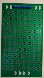
This PCB just arrived. It is the 3rd generation. It is the first PCB that I actually like the layout and the flexibility of using any JFET in any position in the circuit.
Just mounted the terminal blocks. I will install one pair of devices and have a look.
The silk screen lettering is too small but not a reason to re-spin. The resistors should show up tomorrow.
The devices will be J113 and J175 which are available from distributors today.
Just mounted the terminal blocks. I will install one pair of devices and have a look.
The silk screen lettering is too small but not a reason to re-spin. The resistors should show up tomorrow.
The devices will be J113 and J175 which are available from distributors today.
Attachments
Last edited:

Slower? Those of us on the sidelines, rooting you on and trying to learn as we watch!
Keep up the good work!
+1
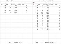
Interesting discovery. After measuring Idss of many JFETs, I am working on identifying some matched pairs for bringing up the PCB with just one or two pairs.
The matched pairs are no longer matched after placing the source resistors. After some trial and error, a good first approximation is to use a 33 ohm source resistor for the J113 and 47 ohms for the J175.
Good thing I am doing this work on a plug-in board.
The matched pairs are no longer matched after placing the source resistors. After some trial and error, a good first approximation is to use a 33 ohm source resistor for the J113 and 47 ohms for the J175.
Good thing I am doing this work on a plug-in board.
> The matched pairs are no longer matched after placing the source resistors.
Maybe you need to match for both Idss and Yfs, or employ the source resistor when you do the matching measurements.
Maybe you need to match for both Idss and Yfs, or employ the source resistor when you do the matching measurements.

> The matched pairs are no longer matched after placing the source resistors.
Maybe you need to match for both Idss and Yfs, or employ the source resistor when you do the matching measurements.
If you look at post 226, I enumerate Rds. Rds ~ 1 / gain. There are no gain matches.
I pulled out a matched pair of Punkydawgs K170/J74. J74 Rds = 32 ohms and K170 Rds = 43 ohms. The ratio of gain N / P for K170/J74 is not 1.
I think that this is one reason you often find a pot as a source resistor in a K170/J74 pair.
> The matched pairs are no longer matched after placing the source resistors.
Maybe you need to match for both Idss and Yfs, or employ the source resistor when you do the matching measurements.
That board looks great Woofertester!
Any idea how long it might take to populate one of these?
Exactly as long as it takes to solder 160 transistors and 240 resistors. If you want to operate as stereo balanced amps, multiply that by 4.
Confirmed 33 ohms as a source resistor for J113 and 47 ohms as a source resistor for J175 gives a good idle current match. I let the JFETs settle at room temperature.
80 cells will yield over 1A idle current per PCB.
80 cells will yield over 1A idle current per PCB.
Rails + / - 12v
One cell populated J113 (D-S-G) with 33 ohm source resistor and J175 (D-G-S) with 47 ohm source resistor
16mA idle current
Output offset <10mV
One cell populated J113 (D-S-G) with 33 ohm source resistor and J175 (D-G-S) with 47 ohm source resistor
16mA idle current
Output offset <10mV
Attachments
Last edited:
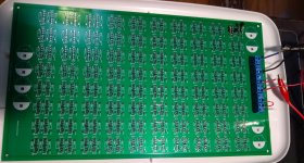
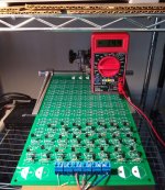
8 cells populated
130 mA idle current. Offset settles to 2 mV. The picture is shortly after power up.
I am bringing this board up one cell at a time to see how it operates.
Ordered some more resistors to have a large quantity of each value for this configuration.
130 mA idle current. Offset settles to 2 mV. The picture is shortly after power up.
I am bringing this board up one cell at a time to see how it operates.
Ordered some more resistors to have a large quantity of each value for this configuration.
Attachments

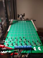
Up to now I have had the input shorted. Removed the short and inserted a 220k resistor. The output snapped to -350 mV. I added J113s until the output went positive. That required 3 J113 JFETs. From now on, I will not have the input shorted as I add cells.
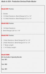
Resistor Lead Bending Tool | Production Devices
Can be interesting tools 3 pcs. 800K kit 🙂 ..Or find some similar model(s) Best regards
Can be interesting tools 3 pcs. 800K kit 🙂 ..Or find some similar model(s) Best regards
Attachments

- Home
- Amplifiers
- Pass Labs
- Beast with 1000 JFETs redux?