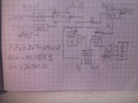
I2S is a Philips standard that to my knowledge 96k 24bit has 48 BCK. this makes 4.5Mhz. Am I wrong? Running the MC at 12v along level shifters, should be enough.
I am looking for a small FIFO to write in 48bit rate but read in 32. By this the DAC doesn't see 12clock bit stopped, and the max ck becomes 3.1Mhz.
A serious I2S PCM adapter looks to be this one.
DocumentDownload/PCMboard at master * iancanada/DocumentDownload * GitHub.
Attachments
Last edited:
I forgot the PCM1702 is 20bit not 24. I must review the circuit, it must stop not 12 but 16ck bits.
Last edited:
I am here really only trying to help you. I asked you for the specific I2S source, because almost any I2S source on the market outputs the data in 64-Bit samples (stereo), in which 16 or 24 bit can fit and the rest bits are zero. This is how the shift registers in my DAC are working and I simulated it here in Quartus. I2S sim
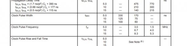
As Marcel said, your "1970's CMOS logic" ... it can safely handle only 5.3 MHz at 15V supply 😱. Your 8.3 MHz is potential performance and not intended for design purposes (as a Designer you should know this). Not me, but the datasheet says that: "Data labelled “Typ” is not to be used for design purposes but is intended as an indication of the IC’s potential performance. "
Now if you calculate 96kHz sample (1 LRCK clock), the BCK speed will be 64 x 96000 = 6.144 MHz. So it can easily happens, that many bits will be skipped and the result of the recording will be popped. Perhaps you can find/create an I2S source with 32-Bit word (stereo, 2x16), but it can be a programming challenge for you.
Another challenge with 15V supply logic is the voltage input and output compatibility (how to balance different voltage levels).
You can take the shift registers from my AD1862 DAC (use 74AHCT164D - it is up to 125 MHz minimum at 5V supply and TTL level logic compatible).
Attachments
A serious I2S PCM adapter looks to be this one.
DocumentDownload/PCMboard at master * iancanada/DocumentDownload * GitHub.
If you use Ian's PCM adapter, you do not need to solve the conversion because there you can connect the PCM1702 directly and the conversion is done in the PCM adapter.
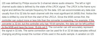
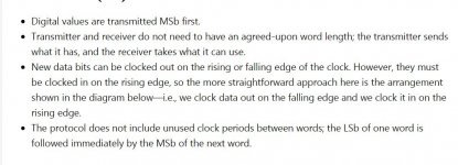
I have always seen a 16bit word I2C to be 32bit never have seen 64. The document of I 2C that what says 8bit to 32bit each channel variable and not fix. This is why it is left justify so that the one which is 8bit, collects the first 8 highest bits and goes deaf until the end LRCK even what is following higher definition bits are still pouring.
May be an expert as abraxalito can shed some light on it.
May be an expert as abraxalito can shed some light on it.
Last edited:
Read the original I2S bus specification from philips:
"When the system word length is greater than the transmitter word
length, the word is truncated (least significant data bits are set to ‘0’)
for data transmission."
"If the MSB follows immediately the LSB, this means 16bit/channel is 32bit."
ee ... there is technically only one MSB and the rest is LSB
64-bit word >> 2x32 bit >> 2x (16a+16b) where 16a is DATA with MSB first and 16b are zero (which can be considered as LSB).
Why don't you take a digital analyzer and look at that I2S data? I did it a few times.
You will spend hours on the wrong design with thinking that BCK frequency is not constant for 16b and 24b recordings in the same LRCK.
How cares what data is truncated and not transmitted.
If the MSB must immediatly follow the LSB of the precedent than you need to delay only one word length to make the two channels simultaneous, 16 or 24 to be selected.
If you have observed the data on scope, than 2×16bit data in 64bit format should see half of the time flat zero, is it the case.
I have seen fix 32bit×2 I2S from asynchronous SRC outputs for any input data length. This what you need to make your DAC work properly.
Or else it will sample the 16bits of right channel, fill with 4 highest bits of the left channel in the 4 lower bits mixing the two channels and repeat to other channel exactly the same copy but 1fs delayed by 32bit shift register.
"I have seen fix 32bit×2 I2S from asynchronous SRC outputs for any input data length. This what you need to make your DAC work properly."
And exactly this is how the most I2S sources are created, with the fixed word (64b is the most common, ... 128, 48, 32 is rare or perhaps selectable in a device). The shift register in my DAC is universal for 16b and 24b recordings (thanks to fixed word length from almost any I2S sources - 64b ... both channels are working correctly - recordings can be audible only in the left channel or only in the right channel - so nothing is mixed).
The question still be what is your I2S source with the 32b word length for 16b recordings or 48b for 24b recordings?
Normal use of DAC is by USB, SPDIF, coaxial/IR, etc, link to CD player PC or may be Internet streaming. All these are normal variable word length. With my double PLL for sync, I don't need any SRC.
If your intention is to be used only by a SRC, there is much simpler way of doing it, Analog devise AN207 document applied to XMOS SRC
AD1862 R2R nonoversampling NOS Audio DAC with FIFO reclock - DIYINHK
discussed here
I2S to AD1862
If your intention is to be used only by a SRC, there is much simpler way of doing it, Analog devise AN207 document applied to XMOS SRC
AD1862 R2R nonoversampling NOS Audio DAC with FIFO reclock - DIYINHK
discussed here
I2S to AD1862
Last edited:
You are right the 16bit I2S is 64bit clock.
Thank you for warning me.
Thank you for warning me.
Attachments
Last edited:
No problem 🙂
Can you come in my thread and fix some facts? Just kidding 😀
I created the stopclock based on AN207, but the LE is controlled by flip flop. I want the LRCK very clean and generated directly from the source .. that is why shift registers won 🙂 The stopclock is worth for TDA1540 (here the additional BCK can be disruptive).
Last edited:
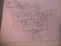
The circuit bellow works as FIFO. The two channels are identical and in parallel ,so one is shown.
The data of 20bit is captured by serial/parallel shift registers using 64fs clock and disabled until the fall of LRCK which passes the parallel data to serial register. The PLL creates a 20fs clock to unload the received data to the delay line and the DACs. The first 16bits are clocked and stopped when the 17th bit arrives on its own delay and by multiplex is guided to the DACs until the 20th bit when the LRCK fall and all restarts again.
By this the 64bit registers are working at 1.9Mhz for 96khz fs. The DACs are working with non stopped 20fs clocks.
I need now make the timings and figure out 16/20bit counters.
Attachments
Last edited:
I am using 74hc40105 FIFOs 2/channel which simplifies the acquisition stage. The input captures the first 20bits of 1 bit delayed DATA controlled by 2×4bit counter, all clocked by 64fs BCK . The read of FIFOs is continuous by 20fs created by sync PLL the serial output is already the finished data, it is shifted sequentially the first 16 by 20fs in 3×16bit shift register followed by the other four shifted in 3×4 shift register. A mux directs the sequential data to the 3 delayed DAC inputs. The second channel is identical, sampling on opposite polarity of LRCK.
If the PLL and only the FIFO part are integrated together, it forms an autonomous I2S PCM sync. converter.
If the PLL and only the FIFO part are integrated together, it forms an autonomous I2S PCM sync. converter.
Attachments
Last edited:
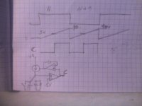
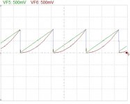
The Ramp Generator.
The ramp generator is the chief orchestra of the interpolator. When it is zero volt at start, the resulting output of the DAC should be the actual sampled voltage, that is nothing should be add. when it reaches 10V the output has gradually interpolated to the next sampled value.
I said 10V and not 1V, because the AD633 multipliers divide the product by 10.
The great challenge, is to have the ramp extremely sharp zero return ready for next sample. Another problem is that my fs is variable to be 44.1khz, 44khz, 96khz, at all speeds the ramp must reach 10V precise at the end of the fs cycle.
The first approach I have for the fast zero return is to use matched pair of capacitors switched alternately charged by a current source. By this when one is charging the other is discharging by shorting switch to be ready for the relay.
To adjust automatically the ramp slope, a comparator looks the ramp comparing to the mid cycle value, 5V. If the ramp is perfect reaching 10V at the end, than the duty cycle of the comparator is exactly 50%. If it is to end higher or lower, the duty cycle is measured by an integrator to feedback the current source and bring it to 50%.
Attachments
Last edited:
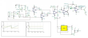
This is the interpolating analog clock generator. It generates a ramp always equal to 1v peak at any input fs frequency as well as the square function of the ramp. In the interpolating formula they are P and P2.
The function is nearly what is described in precedent post except that the capacitors aren't switched but each has its own current source and the two alternating ramps are simply added. It returns to zero in 50ns mainly delayed the opamps but there is still margin as the DAC analog outputs settle in 200ns. The discharging mosfets are arbitrary here, ssm3sk339 in in my mind.
The AD633 low cost multiplier was too slow in zero return and too noisy NF1uv, so I replaced with AD835 200Mhz NF50nv. Unlike the AD633 with fix 1/10 output multiplier, the AD835 is adjustable, so I brought both clocks to 1Vp.
Now all the variables and parameters are ready to form the analog cubic spline calculator.
Attachments
Last edited:
Is there any current sample and hold to reduce I/V glitches while the analog output settles?
I found voltage mode from TI doc. https://www.ti.com/lit/ug/tidu022/t...47933&ref_url=https%3A%2F%2Fwww.google.com%2F
But nothing in current mode.
The PCM1702 has 200ns settling time, for 96khz/20.8us it is 1% only but still one can see on datasheet the distortion increase by sampling higher.
I found voltage mode from TI doc. https://www.ti.com/lit/ug/tidu022/t...47933&ref_url=https%3A%2F%2Fwww.google.com%2F
But nothing in current mode.
The PCM1702 has 200ns settling time, for 96khz/20.8us it is 1% only but still one can see on datasheet the distortion increase by sampling higher.
Last edited:
Why complicate it with deglitching, PCM1702 is considered as glitch-free due to sign-magnitude architecture, ... finding or creating a low THD analog switch for voltage out hold circuitry is hard, because switch has own THD. Controlling the switch with slowed LRCK can increase jitter problem.
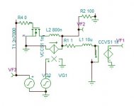
To maintain a current for only 200ns, an inductor should be sufficient, I said to myself.
I made a quick modeling to see the theory in action.

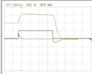
The CCVS simulated the I/V converter 1V/1ma, the current generator was pouring 1ma when it shut off to 0ma. The 200ns following pulse shorts the generator to let the 10uH inductor continue pouring 1ma.

It looks promising, I need to understand why the inductor passes more current in hold time than the sampled one. If I add a gate stopper, the hike increases! strange isn't it.
I made a quick modeling to see the theory in action.
The CCVS simulated the I/V converter 1V/1ma, the current generator was pouring 1ma when it shut off to 0ma. The 200ns following pulse shorts the generator to let the 10uH inductor continue pouring 1ma.
It looks promising, I need to understand why the inductor passes more current in hold time than the sampled one. If I add a gate stopper, the hike increases! strange isn't it.
Attachments
- Home
- Source & Line
- Digital Line Level
- Analog Delta-Sigma interpolation DAC