Is anyone here familiar with Solomon Acko's AK4499 dac, as seen here: AckoDAC based on AK4499EQ
Hi Mark
Given the complexity of today's DACs, I guess the best option for us DIYer is probably to start from an existing board that is already populated where it is delicate to DIY... or even to start from an existing complete unit à la D90 and tune it... or add features.
Both options should be non expensive to remain competitive and avoid ruin in case of failure - not easy I must admit when one sees the cost of some evaluation boards :-(
But let's see what kits and options appear on the market, and how fast the Chinese learn from reading us LOL... unless someone comes with a reasonable GB
Claude
> A few points I'm struggling with - in I/V mode I don't see the advantage of the I/V stage feedback being returned to the die..
You may find this useful :
http://www.easyaudiokit.com/bekkan2019/NewDevice/NewDevice.html
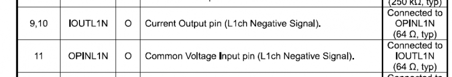
And of course R3 is not 0R, but 64R.
But not important for FET input opamps.
And most likely not important for discrete IV circuits also.
Cheers,
Patrick
.
You may find this useful :
http://www.easyaudiokit.com/bekkan2019/NewDevice/NewDevice.html
And of course R3 is not 0R, but 64R.
But not important for FET input opamps.
And most likely not important for discrete IV circuits also.
Cheers,
Patrick
.
Attachments
> A few points I'm struggling with - in I/V mode I don't see the advantage of the I/V stage feedback being returned to the die..
You may find this useful :
http://www.easyaudiokit.com/bekkan2019/NewDevice/NewDevice.html
And of course R3 is not 0R, but 64R.
But not important for FET input opamps.
And most likely not important for discrete IV circuits also.
Cheers,
Patrick
.
Patrick,
Where did you get the info that R3 is 64R? - if true I wounder why AKM would add 64R in series with the input stage of the I/V stage, this will only add noise...
Patrick,
Where did you get the info that R3 is 64R? - if true I wounder why AKM would add 64R in series with the input stage of the I/V stage, this will only add noise...
John,
64R is the DAC OP impedance (resulting from the paralleling of whatever number of unity weighted resistors). Patrick has merely simulated it as a voltage source in series with a resistor which is the equivalent.
TCD
John,
64R is the DAC OP impedance (resulting from the paralleling of whatever number of unity weighted resistors). Patrick has merely simulated it as a voltage source in series with a resistor which is the equivalent.
TCD
Yes but each DAC array is 110 ohms - so wondering where he got 64 ohms...
Yes but each DAC array is 110 ohms - so wondering where he got 64 ohms...
AFAIK, data sheet says 64 ohms.
AFAIK, data sheet says 64 ohms.
The Datasheet say 110 ohms per DAC array (Page 108 - 10.4. Analog Output), in fact its slightly lower (109.88 ohms) when calculating from current output.
Last edited:
See attached.
There is no additional 64R external to the IC in the recommended IV schematics, as far as I can see.
R2 (Zout) is still 110R, as per datasheet.
Patrick
Patrick,
Thanks for pointing this out - the internal schematics shown later in the datasheet (Page 113, 10.4.3. Feedback loop of External Opamp) indicates Zero ohms (but maybe AKM are hiding this extra resistance for the reason mentioned below):-
Looking closer at the second image of Fig.86 (Idle) looks as if the drawing has been modified (the internal signal lines are drawn in a thicker line as if they have been crudely modified with MS paint or some such) - this would suggest that a design change has taken place since first internal datasheets where drawn up.
It would be good if someone with an AK4499 could measure the IC to verify whats really going on (measure the DC resistance between pins IOUTL1N & OPINL1N etc).
Disclaimer - I'm only "theorizing" what could be the reason behind these connection paths if an internal resistance is present:-
1. Maybe part of a Power-on Mute circuitry that didn't function as intended, and has now been "bypassed"...
2. Possibility of various performance level devices from the same silicon spin (thus the not insignificant silicon NRE costs could then be spread across a range of different device part numbers) - Adding any internal resistance at this node will only serve to reduce the dynamic range performance. The lower spec device would have this extra (detrimental) resistance in the feedback path, it would be bonded out (bypassed) on the higher performance devices...
This "Performance limitation / Part # configuration" is common practice not only in the semiconductor industry, but also in the T&M industry etc. - my Agilent scope is sold with a range of bandwidths - all models use the same PCB design but the input stage current is selected to determine the scopes 3dB point (higher B/W = Higher selling price = higher sales margins from the same NRE costs).
Maybe this was the original plan, but late in the day AKM marketing decided that they needed to Best the latest ESS devices and this "feature" has been disabled atleast on the flagship AK4499...
Last edited:
If it were 0R, then there is no need for this extra pin ?
Patrick
Indeed - as I posted earlier in this thread, I DONT understand the need for these extra pins in the first instance... but they start to make some sense if they where part of a now removed "Power on Mute" circuit or lower range devices' "performance limiter"...
If now Zero ohms, it be better just to parallel them on the PCB and return the feedback path external to the IC (when operating the DAC Array in I/V mode).
I/V Mode removes the Voltage coefficient performance issues with the Silicon resistors used in the DAC Array (and to a lessor degree the RDS-on linearity of the Array switching elements) - a limitation of the CMOS based DAC designs - the same issue is faced with the ESS DAC arrays...
Last edited:
I find the Zout of 110R really low.
That is hardly a current source.
It also means a low Zin of the IV circuit (well below 1R) becomes almost mandatory.
Patrick
Yes, no different than the ESS parts in this regard as JohnW mentioned.
I find the Zout of 110R really low.
That is hardly a current source.
It also means a low Zin of the IV circuit (well below 1R) becomes almost mandatory.
Patrick
For DNR the lower the better!!! - in fact the AK4499 DNR / SNR design's performance barrier (like the ESS devices) is purely limited by the thermal noise of the Array source resistance, hence the the difference between DAC Array source impedance between the ES9028Pro and the ES9038Pro....
The AK4499 in Mono mode has a differential source impedance of 55 ohms - double the ES9038Pros 25 ohms... however the AKM almost makes up for this as its DAC array can operate with over 5V rather then the ESS's 3V3 CMOS process limitation...
AKM seem to have taken better care with the Ground and Power arrangements of the AK4499 - but then the ESS parts are 8 channel DAC's so have to "shoe-horn" more channels into an IC package with a lower pin count - not a good place for the chip designer to be in...
Last edited:
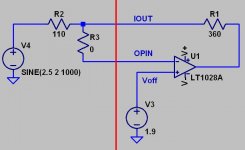
Just for my own interest, as a design challenge.
The IV circuit has been updated with the offset voltage and the equivalent output circuit of the 4499.
This fully demonstrates the importance of a low Zin of the IV circuit.
The complementary MOSFET input solution, with its low Zin, gives a very decent distortion spectrum.
The single ended solution, while much simpler (without the need for the complicated bias circuitry), is 5~10x higher in H2 and H3.
Other so-called discrete solution that I have seen on the net are all using discrete opamps with high Class-A output bias.
I have not found a current-conveyor-based solution as yet.
Not that they do not exist.
Cheers,
Patrick
.
Attachments
Just for my own interest, as a design challenge.
The IV circuit has been updated with the offset voltage and the equivalent output circuit of the 4499.
This fully demonstrates the importance of a low Zin of the IV circuit.
The complementary MOSFET input solution, with its low Zin, gives a very decent distortion spectrum.
The single ended solution, while much simpler (without the need for the complicated bias circuitry), is 5~10x higher in H2 and H3.
Other so-called discrete solution that I have seen on the net are all using discrete opamps with high Class-A output bias.
I have not found a current-conveyor-based solution as yet.
Not that they do not exist.
Cheers,
Patrick
.
Excited to see people working on this!
If it's not too much extra work, would it be possible to also post a jpg of your design?
Just for my own interest, as a design challenge.
The IV circuit has been updated with the offset voltage and the equivalent output circuit of the 4499.
This fully demonstrates the importance of a low Zin of the IV circuit.
The complementary MOSFET input solution, with its low Zin, gives a very decent distortion spectrum.
The single ended solution, while much simpler (without the need for the complicated bias circuitry), is 5~10x higher in H2 and H3.
Other so-called discrete solution that I have seen on the net are all using discrete opamps with high Class-A output bias.
I have not found a current-conveyor-based solution as yet.
Not that they do not exist.
Cheers,
Patrick
.
Sorry, I cannot help as I dont use LTspice so cannot open your files - I find the schematic entry of LTspice to be so hard to use - just plan awful...
- Home
- Source & Line
- Digital Line Level
- AK4499EQ - Best DAC ever