If there was a particular "astuce" it was yours and palstanturhin's knowledge that an LM1875 can be operated well below a gain of 10. At a gain of 3.5, the LM1875 is surprisingly stable. Even most fake LM1875. That means, it was much easier to make more LM1875 work in parallel. Many thanks for that information.I don't understand what "astuce" did you find after two months of research to parallel so easily triple LM1875s.
Next, when building my test-amp I used yours, Turbowatch2's and Nigel's advise of using low impedance connections (it took longer time to do but it was probably worth it). As Nigel once wrote, the feedback resistor and the decoupling capacitors need as short leads as possible. It took some time as well but I believe I managed quite well.
I tested all my fake LM1875 and used three of the best from the same production lot (better chance of equal behavior).
Then a good portion of undeserved luck.
I tried to give my test amplifier as little reason to misbehave (oscillate) as possible and it seems to work out.
Why did it take more than 2 months? Mainly because of family obligations in particular during the Christmas+New Year period, some trivial illness, shortage of 0.33Ohm/5W load balancing resistors. We spent quite some time investigating the nature of the LM1875 (oscillation in particular) and the difference with fakes. I once waited more than an hour for the first dish to be served in a small gourmet restaurant and was told it was normal because the "chef" was an "artist". I will try the same dubious reply here - it took so long because we are "artists".
My guess and hope is that further progress will be more predictable and we again are seen as decent engineers.
Last edited:
In position b , the main issue was offsets and gains of paralleling amps. I see now you have successfully paralleled . But how a DIY will do it. Is he going to cut the outputs and inputs of each amp , apply ground to adjust offset , apply Vref to adjust gain , re link inputs & outputs , repeat for the other branch, adjust offset to balance the bridge , varnish the 13 adjusts. Or you have found an "astuce" for it?Chris and others have put great effort into improving amplifiers based on the LM1875 chip. The results achieved are very promising but evidently limited by the moderate current capability of the LM1875 chip.
In order to overcome the limited current handling of the LM1875, it has been discussed to design a version with more LM1875 operating in parallel such that the current handling is increased. A parallel version may allow for a BTL configured version based on LM1875s with an output power well exceeding 100W. As a last feature, it has been envisaged to use an OP-AMP controlling loop for a composite amplifier design. Composite amplifier designs can achieve very low THD values.
For a start it is foreseen to progress as follows:
a) Discussion of principles and design details, initially of a parallel LM1875 amplifier.
b) Establishment of a design for a parallel LM1875 amplifier.
c) Construction and test of such a parallel LM1875 amplifier.
d) Design of an OP-AMP control loop for the parallel LM1875 amplifier in a composite amplifier configuration.
e) Construction, test and trimming of the composite amplifier.
f) Construction of a similar composite amplifier for a BTL configuration.
g) Test of the composite BTL configured LM1875 amplifier.
h) Eventual PCB layout for those interested.
Anybody is evidently invited to take part, actively or more passively, in this project. It is obviously an objective that the project will end up in a high performance amplifier. But beside that aim, it is hoped that the process will show to less experienced diy’ers what considerations and methods are part of an amplifier design. It should be kept at a level were most members can follow the discussions.

Last edited:
I don't understand what i did (in details), so cannot answer, i don't have the background. I only choosed a shematic/thread wich seems interesting. In electronic, I'm only good at soldering and selecting the parts of the shematic. 😛It looks really good.
LM3886 is more powerfull than both LM1875 and TDA2050. You also use a slightly higher supply voltage.
I notice that the LM3886 is set for an amplification of 22 times (+1) and use an 1/5.7 scaler (divider) before the LM3886 such that you have a resulting gain of 4 from the output of the OP-AMP. We use 3.5 but for less output power/voltage.
Do you know how LM3886 reacts with a gain below 10 times?
Do you know what is the advantage of taking the LM3886 feedback signal after the current detecting resistors (R1/R2)?
I would add a 47K resistor at the very input, before C1, to reduce "plop" from connection/activation of a source while the amplifier is turned on.
At start, I didn't like how Tom wrote on the forum, so i tryed to find something else, more diy.
In position b , the main issue was offsets and gains of paralleling amps. I see now you have successfully paralleled . But how a DIY will do it. Is he going to cut the outputs and inputs of each amp , apply ground to adjust offset , apply Vref to adjust gain , re link inputs & outputs , repeat for the other branch, adjust offset to balance the bridge , varnish the 13 adjusts. Or you have found an "astuce" for it?
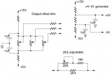
You are right that the adjustment procedure needs re-thinking.
Cutting the outputs to the load balancing resistors is not necessary. The voltages can be trimmed even when they are connected to a common output.
Some DIYers will be able to do adjustment with fixed resistors, some not. For those who prefer trim-pots, I suggest the following circuit modifications (please see the appended sketch).
I see no problem in the input being shorted to ground and each of the three outputs being trimmed to a minimum output voltage. For that I suggest the part of my schematic named "Output offset trim".
Matching of gain will be necessary but requires a 4V test source. Here I suggest the part of my schematic named "+4V/-4V generator".
If two of the three 2K2 input resistors are replaced with the schematic part named "2K2 adjustable", two of the three LM1875 circuits can be gain-adjusted to match the gain of the third.
Are these reasonable solutions for the DIYers that will not be successful with fixed resistor adjustment?
Attachments
Last edited:
I don't understand what i did (in details), so cannot answer, i don't have the background. I only choosed a shematic/thread wich seems interesting. In electronic, I'm only good at soldering and selecting the parts of the shematic. 😛
At start, I didn't like how Tom wrote on the forum, so i tryed to find something else, more diy.
It looks like a fine circuit. I was mainly curious to know what is the advantage of the local LM3886 feedback from the output of the current sensing resistor.
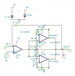
Here is a simpler parallel master+2slaves. The first U1 is autonomous voltage amp to have it's output feed backed , the two others measure the current passing through R1 and pour to the load as much , tripling the output current of the master autonomously .
An artist works with music not with measurements.

An artist works with music not with measurements.
Attachments
Last edited:
It looks like a fine circuit. I was mainly curious to know what is the advantage of the local LM3886 feedback from the output of the current sensing resistor.
Oh...you talk about the remote sensing resistor maybe ? It's to compensate wire resistance. It s a 4 wire output amp ^^
If you build a real amp at the end, it will be a great advantage to select the chips for offset and then arrange them into groups with lowest differences. This reduces the resistor value needed at each chips output and the amount of correcting voltage applied.
If you have a larger number of chips, maybe 15 while 12 needed, from the same production run and non fakes, you should be able to eliminate a large portion of the problem. Also, you get a qualified idea how much correction is needed, instead of estimating based on data sheets.
If you have a larger number of chips, maybe 15 while 12 needed, from the same production run and non fakes, you should be able to eliminate a large portion of the problem. Also, you get a qualified idea how much correction is needed, instead of estimating based on data sheets.
Hi everyone,
great results and progress you guys are posting here! I'm a little occupied with my notch project at the moment, but I'm still following along here 🙂.
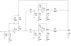
All those problems we're having with LM's not performing to specs, being counterfeits or simply mislabelled TDA's made me think about going back to the first schematic that was posted in this thread by kokoriantz. This circuit is probably not the best performing, but it should be the most forgiving one, while still being better than a plain vanilla 1875. Here's a schematic of a prototype I'm planning to build:

Some of the advantages:
The LM (or TDA or whatever really) is running with 20+ dB inside its specified range (R2/R3, R9/R10). This should work with any part out there, even the cheapest ones without any working protection circuits that are not stable with negative gains.
Output offset is negligible when using capacitors C4 and C5 to AC-couple the feedback path. This makes trimming the whole thing a lot easier. For a more High-End approach, one could easily add a servo circuit at the non-inverting inputs of each LM. This makes the circuit more complicated though. When the servo is not used, R1/R5 and R6/R12 might be omitted.
Only the gains of the LM blocks have to be trimmed via R3 or R10, much like in the Linn circuit that was posted above.
C1 and C2 are needed to make the whole thing stable. The values above work with a simple simulation model. I will see if they hold up in the real world. It would be great to find a one-size-fits-all version that works with genuine and counterfeit parts alike.
R7/R8 set the overall gain of the amplifier. Values below 20dB are easily possible. For extremely low gains like 1x, 2x, 3x etc. the capacitors C1 and C2 may need some further adjustment for stability.
C7 removes the input offset of U3. Again, a servo might be added to remove the even the last mV from the output. I consider this to be overkill though.
Now on to the veroboard and soldering iron 😎!
great results and progress you guys are posting here! I'm a little occupied with my notch project at the moment, but I'm still following along here 🙂.
All those problems we're having with LM's not performing to specs, being counterfeits or simply mislabelled TDA's made me think about going back to the first schematic that was posted in this thread by kokoriantz. This circuit is probably not the best performing, but it should be the most forgiving one, while still being better than a plain vanilla 1875. Here's a schematic of a prototype I'm planning to build:
Some of the advantages:
The LM (or TDA or whatever really) is running with 20+ dB inside its specified range (R2/R3, R9/R10). This should work with any part out there, even the cheapest ones without any working protection circuits that are not stable with negative gains.
Output offset is negligible when using capacitors C4 and C5 to AC-couple the feedback path. This makes trimming the whole thing a lot easier. For a more High-End approach, one could easily add a servo circuit at the non-inverting inputs of each LM. This makes the circuit more complicated though. When the servo is not used, R1/R5 and R6/R12 might be omitted.
Only the gains of the LM blocks have to be trimmed via R3 or R10, much like in the Linn circuit that was posted above.
C1 and C2 are needed to make the whole thing stable. The values above work with a simple simulation model. I will see if they hold up in the real world. It would be great to find a one-size-fits-all version that works with genuine and counterfeit parts alike.
R7/R8 set the overall gain of the amplifier. Values below 20dB are easily possible. For extremely low gains like 1x, 2x, 3x etc. the capacitors C1 and C2 may need some further adjustment for stability.
C7 removes the input offset of U3. Again, a servo might be added to remove the even the last mV from the output. I consider this to be overkill though.
Now on to the veroboard and soldering iron 😎!
Attachments
Here is a simpler parallel master+2slaves. The first U1 is autonomous voltage amp to have it's output feed backed , the two others measure the current passing through R1 and pour to the load as much , tripling the output current of the master autonomously .
An artist works with music not with measurements.
Many thanks for the circuit suggestion.
I notice that for the two current follower amps U2 and U3, the noise gain seems to be 1. Palstanturhin had oscillation phenomena with gains below 3. May such oscillation appear for these current followers as well?
Am I right in that this circuit is quite demanding on the common mode input range for the current followers U2 and U3 as the inputs will swing the amplitude of the U1 output?
Oh...you talk about the remote sensing resistor maybe ? It's to compensate wire resistance. It s a 4 wire output amp ^^
Many thanks for your explanation.
The current amps don't have any voltage gain and they are very stable. They even don't have any ground reference to know at what potential they are flying. Yes the inputs reach the Vee/Vss limits , this why I adjusted the current sense resistors to 0.5 instead of 0.1 so that the master clips before the inputs reach to their limits . With 8 ohms load per IC the output can clip at 22.4v while the current slaves still pouring the same current as the master.
If you build a real amp at the end, it will be a great advantage to select the chips for offset and then arrange them into groups with lowest differences. This reduces the resistor value needed at each chips output and the amount of correcting voltage applied.
If you have a larger number of chips, maybe 15 while 12 needed, from the same production run and non fakes, you should be able to eliminate a large portion of the problem. Also, you get a qualified idea how much correction is needed, instead of estimating based on data sheets.
This is one way to reduce the need for adjustment. This was what I did in part to reduce the risk of mismatch in my triple-LM1875. If there is a possibility that the LM1875/TDA2050 are fake, it is almost a necessity as the production lots perform quite differently.
The slight disadvantage, in particular when screening the ICs, is the need for a test-circuit and some test gear. This may be a problem for some DIYers to whom only the most basic tools are available. I understand the wish to have a version where the use of genuine ICs means the possibility to trim the circuit to good function "as is".
For sure, my suggestions for adjustment take wider tolerances than experienced in practice into account.
Maybe one thought about the output offset, which will always be some mV, resulting from the input that hangs at a small voltage. External DC is successfully blocked by a high quality capacitor.
It is no problem for an amp or loudspeaker to have a little voltage at the output. Something, even like like 100 mV is nothing to be concerned on that side.
The problem arises if parallel connected amps have different offsets and each chip wants to bring the output on it´s level.
If we select the chips for identical offset, this problem is minimized, if we presuppose that identical produced objects, mounted on one heat sink will have an identical thermal drift. So we come to matching chips.
*This selecting of parts for some parameter is often made in the voodoo corner of hifi, as it brings some individuals in the favorable situation to virtually sell air for big money.*
Here it has real advantages, as you can minimize the value of the resistor that is supposed to flatten out this problem. One advantage of paralleling chips or transistors, what it is we really do, is the lower output resistance. If we need to increase a resistor to reduce an others resistance, this gets questionable.
Even as individual, active circuits can steer the inputs to zero volt automatically, I would prefer the simpler approach to select chips and then adjust them to 0 volt with a pot.
PS To match the chips a simple eBay amp, upgraded with a Textool socket should be fine. Not even a heat sink needed, if voltage is keep reasonable.
Last edited:
All circuit suggestions most wellcome!
If one can prototype and show results, even better.
I will try put the booster transistors to my proto this weekend and see what happens.
There should be no need to adjust or match anything with that topology at least.
Should be very diyer friendly...
If one can prototype and show results, even better.
I will try put the booster transistors to my proto this weekend and see what happens.
There should be no need to adjust or match anything with that topology at least.
Should be very diyer friendly...
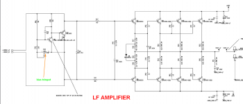
You only need to adjust the series resistor to decide up to what power the IC will work in solo . The circuit bellow, the two last pairs start working above 2A for example. I simulated with the composite you used , I saw no any anomalies when the transistors activate, although I chose slowest ones . Of course c5200/a1943 are still much faster ones if you detect any wrong doings .All circuit suggestions most wellcome!
If one can prototype and show results, even better.
I will try put the booster transistors to my proto this weekend and see what happens.
There should be no need to adjust or match anything with that topology at least.
Should be very diyer friendly...
Attachments
...........................................................
All those problems we're having with LM's not performing to specs, being counterfeits or simply mislabelled TDA's made me think about going back to the first schematic that was posted in this thread by kokoriantz. This circuit is probably not the best performing, but it should be the most forgiving one, while still being better than a plain vanilla 1875. Here's a schematic of a prototype I'm planning to build:
Some of the advantages:
The LM (or TDA or whatever really) is running with 20+ dB inside its specified range (R2/R3, R9/R10). This should work with any part out there, even the cheapest ones without any working protection circuits that are not stable with negative gains.
Output offset is negligible when using capacitors C4 and C5 to AC-couple the feedback path. This makes trimming the whole thing a lot easier. For a more High-End approach, one could easily add a servo circuit at the non-inverting inputs of each LM.
Only the gains of the LM blocks have to be trimmed via R3 or R10, much like in the Linn circuit that was posted above.
C1 and C2 are needed to make the whole thing stable. The values above work with a simple simulation model. I will see if they hold up in the real world. It would be great to find a one-size-fits-all version that works with genuine and counterfeit parts alike.
R7/R8 set the overall gain of the amplifier. Values below 20dB are easily possible. For extremely low gains like 1x, 2x, 3x etc. the capacitors C1 and C2 may need some further adjustment for stability.
C7 removes the input offset of U3. Again, a servo might be added to remove the even the last mV from the output. I consider this to be overkill though.
Now on to the veroboard and soldering iron 😎!
Hi Lasse,
A nice circuit for test!
It is close to the circuit Chris tested but with a controlling OP-AMP loop.
Using the LM1875 with a gain of 10 should make almost any LM1875/TDA2050 work, even the fake ones. With increased LM1875 gain, you will get a little more noise but that is not serious as I see it.
With 10 times LM1875 gain, you push the OP-AMP amplitude working point towards higher THD but also that is not a serious problem. You can eventually adjust your R1/R5/R6/R12 for a lower effective gain.
Your conclusion on the off-set reducing effect of C4 and C5 seems right but at the same time they may cause some problems if any. My fear would be that these capacitors, if triggered by a low frequency signal, could cause a momentary output voltage difference at the two amplifier outputs because the return to balance is slow due to the size of these capacitors. That could be what happened for Chris. Due to the higher gain (10x), matching of gains is more important and due to the capacitors you have to match the gain with an AC signal which is more cumbersome and perhaps less precise. You only need to adjust one gain to match the other as the exact gain is of no importance. I am curious to see if these capacitors give you problems.
For the rest, I have no comments. A good year ago I made some composite amplifier tests with single LM1875. For these tests, adding C2 would only make the whole thing oscillate.
I fully agree with your "one-size-fits-all" approach and at least for now keep it simple and avoid DC-servo's if not really mandatory. There I fully support Turbowatch2's view that bothering about a few Milli-volts is exaggerated.
I very much look forward to hear about your experiences.
NB: You mention a "Linn circuit". Which one is that?
Last edited:
All circuit suggestions most wellcome!
If one can prototype and show results, even better.
.........................................................

It is not that parallel LM1875 is necessarily the best choice. Actually, I assume that there is better. We started with LM1875 out of convenience and I believe we have gained very useful information about its behavior and limits. I will continue that branch because I am already well on my way with that concept.
Anybody else who feels like constructing a power part that preferably can operate from a symmetrical supply is very appreciated. Please provide a schematic and test results so we have a selection to choose from depending on skills acquired, power needed and budget.
The OP-AMP part seems more predictable as long as the power part is reliable. Remember that the power part (amplifier) has to be DC-coupled for the best results.
Yesterday, I studied all chip-amps I could think of to find out why the LM3886 is so popular. My conclusion was that it has by far the highest output current limit, good supply range, it is reasonable in price and as a further advantage has a low THD though not a primary concern.
Last edited:
Maybe you missed my post #398, where I showed how Linn paralleled two TDA1514A in the Majik, and discussed this.
You only need to adjust the series resistor to decide up to what power the IC will work in solo . The circuit bellow, the two last pairs start working above 2A for example. I simulated with the composite you used , I saw no any anomalies when the transistors activate, although I chose slowest ones . Of course c5200/a1943 are still much faster ones if you detect any wrong doings .
The heavy duty version!

- Home
- Amplifiers
- Chip Amps
- LM1875 in parallel configuration and used in a composite amplifier.