This means the input capacitance is not the one causing the second pole as is the case with LM3886 . The sim model to be considered exact.That's looking really nice, much better than my results! Adding some pF across the feedback resistor just made things worse. Makes me think that my LM1875 are anything but genuine... or that my prototype is sufficiently insufficient 😱.
The non-inverting version with lowered resistor values (100/180) is pretty much the same.
EDIT: Here's another thread with a familiar looking circuit in the first post: Composite LM1875 stability issues
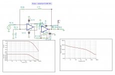
Now with real data , I simulated the circuit which gives the result without 120p feedback capacitor. The frequency response shows the phase shift of 110° occurs at 635khz , for final phase margin of 70° . This is the fastest and frequency the composite amp can have . As the final gain is 20db , the power stage providing 6db , the op amp must deliver at 635Khz 14db. This means the op amp must have 0db gain at 3Mhz . In order to keep a phase margin of 70°, the op amp must have it's second pole above 6Mhz . It is the case with NE5534 proposed. The NE5534 has compensation capacitor , if adjusted to 82pf the simulator shows 3Mhz response. closing the loop gives the expected result . In this option where the op amp provides the dominant pole ,the distortion of the power amp is negligible compared to the open loop op amp's. By this the simulated distortion noise number is nearly exact, 0.00016%.
Attachments
Nice; great performance out of jellybean parts, just the way I like it! Hopefully this holds true with a built and tested prototype...
FF, can you apply a pot. From input to output and adjust for null to see the shape of the distortion for 1 kHz 1W. Joyeux Noël.
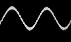
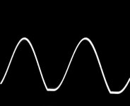
I believe this is what you want: 1W/1KHz in 10 Ohm (9Vpp), 10K pot from input to output, pot-mid trimmed to minimum 1KHz signal. Signal shown is from potentiometer mid-terminal.
15mVpp signal is shown. I guess the 1KHz can only be trimmed fully out if the output is exactly 180 degrees out of phase with the input signal?
Attachments
Many thanks to kokoriantz for the simulation. If we can beef the LM1875 power handling up with more in parallel and reduce the THD+N to something of the order calculated, I believe we have a good "poor mans choice".
As alternative to a parallel LM1875 power block, I am contemplating bread-boarding a buffered LM1875 stage. It can handle about the same current as three parallel LM1875 but is somewhat simpler in implementation and avoids power loss in load balancing resistors. The extra base-emitter voltage drop in the power transistors is compensated in part by less loading of (and voltage drop in) the LM1875. The disadvantage may be slightly increased THD.
This simple class B buffering of the LM1875 was suggested by a member who, if 'm not mistaken, had inspiration from a Quad design engineer.
NB: One clear effect of Christmas is very rapid access to the forum. Probably the same with an important world-wide football/soccer match.
Attachments
Last edited:
This is the distortion image 50mv scale of tda7293 given 0.005%. You can notice the very low level of crossover distortion in your image compared to tda7293 .I believe this is what you want: 1W/1KHz in 10 Ohm (9Vpp), 10K pot from input to output, pot-mid trimmed to minimum 1KHz signal. Signal shown is from potentiometer mid-terminal.
15mVpp signal is shown. I guess the 1KHz can only be trimmed fully out if the output is exactly 180 degrees out of phase with the input signal?
Attachments

This is the distortion image 50mv scale of tda7293 given 0.005%. You can notice the very low level of crossover distortion in your image compared to tda7293 .
Yes, to me the LM1875 distortion looks fine. I just could not trim the 1KHz signal better out. I see the small cross-over "bumps" and compared to the 9Vpp output signal they are very modest.
Thanks for letting me know about this "balanced bridge" type of distortion analysis.

Now with real data , I simulated the circuit which gives the result without 120p feedback capacitor. The frequency response shows the phase shift of 110° occurs at 635khz , for final phase margin of 70° . This is the fastest and frequency the composite amp can have . As the final gain is 20db , the power stage providing 6db , the op amp must deliver at 635Khz 14db. This means the op amp must have 0db gain at 3Mhz . In order to keep a phase margin of 70°, the op amp must have it's second pole above 6Mhz . It is the case with NE5534 proposed. The NE5534 has compensation capacitor , if adjusted to 82pf the simulator shows 3Mhz response. closing the loop gives the expected result . In this option where the op amp provides the dominant pole ,the distortion of the power amp is negligible compared to the open loop op amp's. By this the simulated distortion noise number is nearly exact, 0.00016%.
Maybe build this design and test? All components are layout on standard perfboard spacing. I have also added some parts:
- output zobel network
- decoupling capacitors for the NE5534 and the LM1875
- input capacitor
- resistor bewteen signal ground and power ground
Attachments
I established the LM1875 circuit from the composite amplifier article with the purpose of understanding the open loop transfer function. I used the closest standard resistor values with my signal generator as the output of the AD711 and no feedback loop, evidently.
The sine-wave as such is not as distorted as I would expect but the output signal drifts within 2-3 seconds from one supply rail to the other supply rail. This means the LM1875 has no DC stability and the output DC component is serious. Such can evidently be remedied by an AD711 control loop but requires an AD711 for each LM1875 (such as shown in the article). Then the circuit becomes rather cumbersome. Another problem is that the gain of the LM1875 is in the order of 50 (taking the input divider into account). With such a high gain in the LM1875, the working amplitude of the OP-AMP is so low that the THD of the OP-AMP is not the best.
For these two reasons, the article use of the LM1875 is discarded as a less feasible option.
Output wave-forms are at 1KHz (25Vpp) and show the situation just after start and some 3-4 seconds later.
Attachments


Last edited:
Maybe build this design and test?......
You are fully right, this is one purpose with this project.
I still propose we discuss a little longer on the parallel LM1875 power block that ensures we have sufficient current capability to handle higher power levels than for a single LM1875.
Knowing that the power block works well and the gain of the power block, we can design and test a controlling composite amplifier loop with that power block.
If anyone prefers progressing faster and already now test the controlling OP-AMP loop with a single LM1875, please do so. When you show results, please show exactly what was your test circuit.
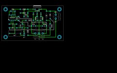
I will work on Vero-board. A real PCB layout I find premature at present. There will be important adjustments of the circuit.
This means the LM1875 has no DC stability and the output DC component is serious. Such can evidently be remedied by an AD711 control loop but requires an AD711 for each LM1875 (such as shown in the article)
What if you put two LMs in parallel, each with a current sharing resistor on the output, and then close the AD-loop around both of them?
What if you put two LMs in parallel, each with a current sharing resistor on the output, and then close the AD-loop around both of them?
My feeling is it will not work like that. Each LM1875 will require a unique DC signal on the input to have no significant DC at the output. A single AD711 may satisfy the need for one of the two LM1875s to have no output offset but the other LM1875 will hardly be satisfied and, due to rather high gain, show a significant DC component. I believe this is what the designer from the article realized so he ended up with one AD711 per LM1875 just to keep the LM1875 operational.
I believe this is what the designer from the article realized so he ended up with one AD711 per LM1875 just to keep the LM1875 operational.
Sounds reasonable 😱
FF, look at post 113. I show the open loop function of the article's circuit . You see the phase at 180° . But , using AD8008, in wide band amplifier, the phase shift remains flat 90°, hence stable . TPA3116D2 has in it two integrators in cascade, de phasing 180° in ac 0° in dc, the same as the article's circuit . By using an all pass filter in between the two integrators, with sim it works , but in real world it behaved the same as you got , unstable operating point. Bruno Pulitzer, probably the author of TPA3116, has patented a fourth order by 4 integrators where the ac and the dc get 0° phase shift . Someone on eebloge has tried it out , his problem is at saturation sticking.
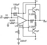
I simulated your idea of output transistors. Using TIP3055/2955 I get the same results as without . Bridged , it can deliver 150W/8 ohm as the unloaded 1875 can be powered 54v to pour +/-50v to the load.
Your layout is not the best. Look at the length of the gnfb loop. You could move the 9K resistor between botk 2k2 resistors and th 82pF cap as a "quick fix" but still not optimal...Maybe build this design and test? All components are layout on standard perfboard spacing. I have also added some parts:
- output zobel network
- decoupling capacitors for the NE5534 and the LM1875
- input capacitor
- resistor bewteen signal ground and power ground
Your layout is not the best. Look at the length of the gnfb loop. You could move the 9K resistor between botk 2k2 resistors and th 82pF cap as a "quick fix" but still not optimal...
You are right about the feedback resistor. Also made some more small changes.
Attachments
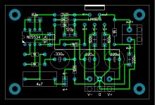
Be much more generous with the track output to + speaker. If cannot have whole pours for +V&-V make the link as straight as possible so that a DIY can parallel upon the track, thick cooper wire. You must add a 10k grounding the + input of NE5534 , as you added a capacitor. The 1k resistor in series with 4.7u is useless.You are right about the feedback resistor. Also made some more small changes.
Last edited:
- Home
- Amplifiers
- Chip Amps
- LM1875 in parallel configuration and used in a composite amplifier.