Hello Mr. Pass,
I gave the H2 you kindly gave to me at BAF to a young fellow who couldn't attend, and who is developing into a DIY nut.
May I buy another one for myself, please?
Thank you,
Greg
I gave the H2 you kindly gave to me at BAF to a young fellow who couldn't attend, and who is developing into a DIY nut.
May I buy another one for myself, please?
Thank you,
Greg
Perhaps there is some confusion. The Vp on the J112's is achieved by
placing +12 on the Drain, grounding the Gate and using 1 megohm
series resistance from Source to Ground. The Vp is the resulting voltage on the Source pin. The Drain current is a couple microamps.
This is used to decide what the rail V+ voltage should be on the supply
voltage at the test points as referenced by the curves in the article.
Thanks Mr. Pass for your clarification. It works. I understand to go to the last graph which is entitled "Calibration of T2 vs Vp Pinch Off Voltage" in the revised article.
1. Match the number which was written on the envelope by PASSWORKS to the number on the X axis. My number is 2.79
2. Draw a line perpendicular to the X-axis at point 2.79 and have it intersect the 1% H2 distortion line; call it point A.
3. I draw another line which is parallel to the X-axis which also intersects at point A. The other end of this horizontal line terminates on the Y-axis at point B. The voltage at point B reads 16 V.
4. Adjust the potententiometer [P1 and P2] so as to get a value of 16 V at test point T2.
I now have a calibrated and authentic stereo 1% H2 distortion generator. And I am very happy!
Best
Anton
Just remember that the calibration is not very exact. Those who wish exact
figures will need to use a distortion analyzer.

figures will need to use a distortion analyzer.
How does the H2 generator work?
Thanks Mr. Pass for your advice. I am fully satisfied that H2 is ~at 1%.
I continue to study your articles on H2. I 've come to understand how this generator works and/or its mechanism for H2 sysnthesis as follows:
1. As shown in the schematic, FET operates as a constant current source.
2. But; as the AC [music] signal goes positive at the gate relative to source, FET works as an enhancement device; because its P-N junction becomes forward biased. FET amplifies this positive-going input. The resultant amplified output at its drain is negative-going or phase inverted.
3. As the music signal goes on to be negative-going at the FET's gate relative to its source, the FET now works in a depletion mode. The resultant output at the drain port is positive-going.
4. FET is the simplest DEF; this one with voltage gain; it operates in both depletion and enhancement modes.
5. But; what if the voltage gain in the enhancement mode is more than that in its depletion mode. This [actual] assymetry in amplifiying the positive going and negative segments of music causes the H2 distortion; relative to the fundamental at the gate port.
6. The PASSWORKS data suggest that the voltage gain in the depletion mode is less than the voltage gain in the enhancement mode. Meaning the positive going signal at the FET's drain is lower in absolute magnitude than its negative-going signal. This is H2 negative phase as described by Mr. Pass. Sounds like it is "easier" for the FET to enhance that to deplete.
Best
Anton
Just remember that the calibration is not very exact. Those who wish exact
figures will need to use a distortion analyzer.
Thanks Mr. Pass for your advice. I am fully satisfied that H2 is ~at 1%.
I continue to study your articles on H2. I 've come to understand how this generator works and/or its mechanism for H2 sysnthesis as follows:
1. As shown in the schematic, FET operates as a constant current source.
2. But; as the AC [music] signal goes positive at the gate relative to source, FET works as an enhancement device; because its P-N junction becomes forward biased. FET amplifies this positive-going input. The resultant amplified output at its drain is negative-going or phase inverted.
3. As the music signal goes on to be negative-going at the FET's gate relative to its source, the FET now works in a depletion mode. The resultant output at the drain port is positive-going.
4. FET is the simplest DEF; this one with voltage gain; it operates in both depletion and enhancement modes.
5. But; what if the voltage gain in the enhancement mode is more than that in its depletion mode. This [actual] assymetry in amplifiying the positive going and negative segments of music causes the H2 distortion; relative to the fundamental at the gate port.
6. The PASSWORKS data suggest that the voltage gain in the depletion mode is less than the voltage gain in the enhancement mode. Meaning the positive going signal at the FET's drain is lower in absolute magnitude than its negative-going signal. This is H2 negative phase as described by Mr. Pass. Sounds like it is "easier" for the FET to enhance that to deplete.
Best
Anton
Last edited:
Nelson,
I recall you mentionned to having to go through a non negligible amount of jfet to find those with the suitable Vp.
Might I ask what the average yield was for you, say for a batch of 1000 ?
Just wondering...
Thanks,
Max
I recall you mentionned to having to go through a non negligible amount of jfet to find those with the suitable Vp.
Might I ask what the average yield was for you, say for a batch of 1000 ?
Just wondering...
Thanks,
Max
I recall you mentioned to having to go through a non negligible amount of jfet to find those with the suitable Vp.
Might I ask what the average yield was for you, say for a batch of 1000 ?
First, it was limited to J112 only. Of that, maybe 25% were in the range
2.5 - 3.0 Vp that fit the application.
First, it was limited to J112 only. Of that, maybe 25% were in the range
2.5 - 3.0 Vp that fit the application.
Thank you!
Not as bad as I thought though... not counting labour time/cost of course! 🙂
2. But; as the AC [music] signal goes positive at the gate relative to source, FET works as an enhancement device; because its P-N junction becomes forward biased. FET amplifies this positive-going input. The resultant amplified output at its drain is negative-going or phase inverted.
The gain of the Jfet in this circuit is nearly 10, and the Gate starts to
conduct at Vgs at about +.6V. This being the case, you will be into
positive Gate current with the output somewhere around -6 volts,
which is well past clipping.
The gain of the Jfet in this circuit is nearly 10, and the Gate starts to
conduct at Vgs at about +.6V. This being the case, you will be into
positive Gate current with the output somewhere around -6 volts,
which is well past clipping.
Thanks Mr. Pass for your comment. You inpired me to do this following experiment with my H2 Preamp V1 [H2 V1]. The purpose is to understand the synthesis mechanism of H2. Maybe useful for calibration and matching the two channels.
1. The useful and suggested output of [H2 V1] is 1 V rms. This the same as 2.8 V peak to valley of the AC signal.
2. [H2 V1] has a voltage gain = 10. So the input signal at the gate of JFET is 0.28 V peak to valley. Or +0.140 V peak at the gate relative to the source which is at zero volts. My supposition is its positive-going value causes the FET to operate in the enhancement mode.
3. The minimum value of the signal's valley is -0.140 V at the gate relative to the source which is still at zero V. My supposition is the FET now operates in depletion mode.
4. [H2 V1] is a DC and an AC amp. I can easily drive its gate with a +/- 0.140 Vdc. And note the resultant voltage drop across the load resistor. Will this voltage drop across the drain resistor at a [+0.14 V] gate drive be equal in value across the same resistor due to biasing the gate at [-0.140 Vdc instead]?
I have already inserted [H2 V1] between my SONY CD player and my Threshold S/150 power amp. The resultant sound [c/o ADS L730s] due to H2 negative phase is highly detailed, delicate; dancing and very satisfying. I still have to reverse the leads of the speakers for sjubjective comparison.
Best
Anton
4. [H2 V1] is a DC and an AC amp. I can easily drive its gate with a +/- 0.140 Vdc. And note the resultant voltage drop across the load resistor. Will this voltage drop across the drain resistor at a [+0.14 V] gate drive be equal in value across the same resistor due to biasing the gate at [-0.140 Vdc instead]?
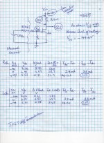
The attachment describes the circuit I used to study the JFET; in order to understand the synthesis mechanism of its resultant H2. I had fun learning/analyzing it.
1. JFET operates as a DC amplifier
2. A 1.5Vdc [AAA battery] and a series-connected resistor [330 K] generate a [ +144 mV] bias voltage at the gate of JFET [Vgs]. A [Vgs = -144 mV] is obtained by reversing the leads of the battery in the same circuit.
3. The two values of Vgs = +/- 144 mV are frozen snapshots of the AC signal at its peak value and at its minimum value.
4. The two tables show the resultant voltage measurements in the circuit for the Right and Left channels. I am seeking matching data!
5. Delta V is the voltage drop across the 332 load resistor at the drain port of JFET. I calculate the drain current by dividing this Delta V by the load resistor.
6. The calculated results in the last two right columns are the significant answers. They effectively say that for either channel; focus L ch :
6a. A value of 2.4 mA is calculated by subtracting drain current at Vgs= 0 from the drain current due to Vgs=-144 mV. I then calculate a value of 0.80 V by multiplying 2.4 mA by 0.332 K load resistor. The resultant value of [0.80 V] is the absolute minimum value of the "equivalent" AC signal.
6b. A value of 2.6 mA is calculated by subtracting the value of drain current due to Vgs = +144 mV from the drain current due to Vgs = 0. I then calculate a value of 0.86 V by multiplying 2.6 mA by the value of 0.332 K of the same load resistor. The resultant value [0.86 V] is the peak value of the equivalent AC signal.
6c. I carefully draw a sine AC signal which has a resultant peak amplitude = [0.86V]; due to its positive- going segment in the time frame of 0 to T arbitrary. I carefully measure the area under the curve of this segment and call it A+.
6c. I continue drawing the negative-going segment of the AC signal which bottoms at [- 0.8 V]. The resultant area under the curve of this segment spanning the later time T to T1 is called A-.
6d. The area A+ is larger than the area A-. This is exactly the teaching of Mr. Pass in his H2 article:
1. {The input signal to JFET [Fundamental] has the area under the curve of its positive segment equal to the area of its negative segment.}
2. { Any difference between the area of the positive and negative segments is called H2; or a Fundamerntal frequency that is enriched with an internally synthesized low level double the frequency of the parent.
3. {I described in my example an H2 Positive Phase}.
The above verbiage is distilled in this simple statement:
The transconductance of this JFET during the positive Vgs drive is larger in value than the transconductance of this JFET during its negative Vgs drive. It has a non-linear amplification.
Best
Anton
Attachments
Last edited:
Hi,
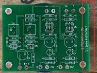
I’d like to slide my H2 into a 75mm wide Hammond case. To do that I’ll need to trim down one edge of the pcb..
This case:
http://www.hammondmfg.com/pdf/1455K1201.pdf
Appears OK to me. Just cutting off 2 mounting holes and their ground connection. Opinions? Other than “shame to cut off the label...”
I’d like to slide my H2 into a 75mm wide Hammond case. To do that I’ll need to trim down one edge of the pcb..
This case:
http://www.hammondmfg.com/pdf/1455K1201.pdf
Appears OK to me. Just cutting off 2 mounting holes and their ground connection. Opinions? Other than “shame to cut off the label...”
Attachments
Last edited:
Looks OK to me Roo2, looks like you are cutting off 5mm to suit the 75mm slot width in the Hammond Box - they are nice small enclosures by the way. No other pcb tracks will be interfered with it seems. Go for it I say.
Are you getting that locally or from an OS source?
Cheers,
Gary..
Are you getting that locally or from an OS source?
Cheers,
Gary..
Thanks Gary. For one off purchases I tend to buy locally from RS Components. Free shipping on everything tends to outweigh the discount available from an OS source.
Just over $30.00 AUD from either RS or Element 14 here in Oz plus freight.
$25.00 AUD from Arrow with free delivery from the US for orders over $50.00 USD. So if you need some other components, then an order to them is worthwhile. Mouser is much the same but minimum $60.00 AUD order value for free FedEx delivery. I buy most if not all parts from either of those 2 suppliers. Arrow, can be very cheap at times on semi's, pays to shop around. For instance,I got some Infineon IRFP150 Mosfets (ZM's favourite) from Arrow at less than half Mouser's price 2 weeks ago.
Cheers,
Gary..
Just over $30.00 AUD from either RS or Element 14 here in Oz plus freight.
$25.00 AUD from Arrow with free delivery from the US for orders over $50.00 USD. So if you need some other components, then an order to them is worthwhile. Mouser is much the same but minimum $60.00 AUD order value for free FedEx delivery. I buy most if not all parts from either of those 2 suppliers. Arrow, can be very cheap at times on semi's, pays to shop around. For instance,I got some Infineon IRFP150 Mosfets (ZM's favourite) from Arrow at less than half Mouser's price 2 weeks ago.
Cheers,
Gary..
Noted. Thanks for the tip.