Do you think degenerating the Q16 of the CCS for the VAS could affect the peaking? I degenerated Q14 and the oscillation did not go away.
EDIT: I'm wondering too if a base stopper between Q16 and emitter of Q14 is necessary.
Hi drinkingcube, simulation shows no impact degenerating Q16 has to the loop gain plot.
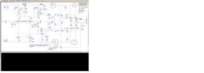
By the way to answer you question about the RC filter on the power rails, it seems to be a common practice to add filtering like the screenshot to the front end supplies.
Attachments
Do you think degenerating the Q16 of the CCS for the VAS could affect the peaking? I degenerated Q14 and the oscillation did not go away.
EDIT: I'm wondering too if a base stopper between Q16 and emitter of Q14 is necessary.
The voltage drop across the 20R is negative feedback into the base of Q14 reducing the Vbe.
sgrossklass commented about the high level of current in the input stage which still applies. In terms of juice it allows over indulgence on the part of Q14.
You will have to hack your pcb to incorporate the 20R or base stopper resistors. That would not be necessary if the current levels in the input stage are moderated.
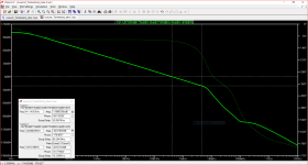
I have looked at this with an increase in output stage standing current - the resultant plot is attached. See what you think.
At a practical level constant current circuits have good supply rejection and you have these in your positive rail.
The charge carriers in a transistor travel from the emitter to the collector and you have a number of these connecting to and exposed to the negative rail which will see switching artefacts from your output transistors.
You need to have some mitigation especially if you are dealing with 10kHz square wave tests.
An RC filter for the small signal negative rail section of 100R plus 100uF would be sufficient.
Attachments
That's what I suspected, I didn't see a change in the loop gain or frequency response plots when I degenerated it. I see what you're talking about now with the RC filter. After noticing that it has to go after the output stage, only for the sensitive circuitry, I realize I would have to tear up a trace. I realize this after I've gone through and looked at the different nets in KiCad and seen how complicated it would be to attach all those leads to one singular point (if that makes any sense). I'm going to seriously consider tearing up a trace, but I'd rather not mangle the board if I don't have to.Hi drinkingcube, simulation shows no impact degenerating Q16 has to the loop gain plot.
By the way to answer you question about the RC filter on the power rails, it seems to be a common practice to add filtering like the screenshot to the front end supplies.
Hmm... So maybe you're suggesting only implementing the RC filter on the negative rail, right before the sensitive circuitry. I'll think about this.The voltage drop across the 20R is negative feedback into the base of Q14 reducing the Vbe.
sgrossklass commented about the high level of current in the input stage which still applies. In terms of juice it allows over indulgence on the part of Q14.
You will have to hack your pcb to incorporate the 20R or base stopper resistors. That would not be necessary if the current levels in the input stage are moderated.
I have looked at this with an increase in output stage standing current - the resultant plot is attached. See what you think.
At a practical level constant current circuits have good supply rejection and you have these in your positive rail.
The charge carriers in a transistor travel from the emitter to the collector and you have a number of these connecting to and exposed to the negative rail which will see switching artefacts from your output transistors.
You need to have some mitigation especially if you are dealing with 10kHz square wave tests.
An RC filter for the small signal negative rail section of 100R plus 100uF would be sufficient.
I'll also take a look at using less input stage Ic.
EDIT: I've stepped the resistor for setting Ic in the input stage of values like 100 140 220 330, and I'm not seeing any difference in peaking or anything in the loopgain plot.
Last edited:
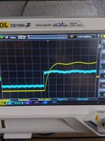
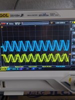
Not sure I'm alone or not but this scope shot has puzzled me,
https://www.diyaudio.com/forums/att...91d1569867713-ringing-img_20190930_112054-jpg
The ringing frequency appears to be nowhere near 16MHz, it is too low a frequency to count 1,600 cycles of it per one 10 KHz square wave period, as would a 16MHz frequency. The ringing ought to be something the loop gain plot does not show us.
Hmm... that's a good point to ask ourselves, would 16 MHz be visible on the square wave? I guess not really, in this case.Not sure I'm alone or not but this scope shot has puzzled me,
https://www.diyaudio.com/forums/att...91d1569867713-ringing-img_20190930_112054-jpg
The ringing frequency appears to be nowhere near 16MHz, it is too low a frequency to count 1,600 cycles of it per one 10 KHz square wave period, as would a 16MHz frequency. The ringing ought to be something the loop gain plot does not show us.
I think I was kind of viewing it like, "the 16 MHz oscillation is obviously there, so SOMETHING must be oscillating so if I fix the 16 MHz oscillation hopefully the square wave response would look better."
Hmm.. That's a good point as well. In a little bit, or next time I'm working on the amp right next to me, I'll attach another scope and show both input and output, maybe there's something hidden there.What does your input waveform look like? Just curious....

Haha, my sim is showing a perfect response as well 🙂Transient analysis with 0.2Vp-p square wave. the output waveform is flawless😀 no ringing, no 16MHz. 😀
I'm powering the amp off two bench supplies, and I'm not sure if that could introduce ringing at all, but I'm wondering if maybe the issue would go when I build the PSU.
After I do this random processes note taking I'm going to fire it up, put an 8 ohm load on it, and see if I'm still getting the weird behavior from the square wave, maybe even see if it goes unstable with some capacitance across the load as well (at low output levels - for safety).
Going to talk to my mentor on Friday and see if he recommends ripping up a trace on the negative side and adding a quick and dirty RC filter to see if that helps.
EDIT: Very intersting, I'm seeing almost the EXACT same 16 MHz oscillation at the input, with nothing on input or load (other than oscope)
Last edited:
I'm sorry, R4 is connected to DIFFGND and GND through the ground plane. GND through the ground plane refers back to the power supply. Am I understanding what you are saying correctly?
Measure the resistance between DIFFGND and GND, if it is not zero, you are doing it wrong.
I am not sure if it contributes the ring. There is a quick test you can run.
Short R4 with a wire. Then, run square wave test again.
Just measured, it's 0.2 ohms.Measure the resistance between DIFFGND and GND, if it is not zero, you are doing it wrong.
I am not sure if it contributes the ring. There is a quick test you can run.
Short R4 with a wire. Then, run square wave test again.
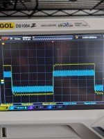
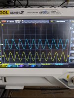
Interesting stuff from looking at the input as well, going to edit this post with pictures in a sec.
Left to right: (blue - input, yellow - output)
1. 8 ohm load, scope on input, scope on output
2. 8 ohm load, scope on input, function generator on input, scope on output
3-4. 10 kHz square wave, 8 ohm load, scope on input, scope on output, 3 is a triggered view, 4 is scope just running normally
Attachments
Last edited:
Normally, without input signal, you will not see signal on input (+). I suspect your current source for long tail pair is not stable.
Hmm... that's a good point to ask ourselves, would 16 MHz be visible on the square wave? I guess not really, in this case.
I think I was kind of viewing it like, "the 16 MHz oscillation is obviously there, so SOMETHING must be oscillating so if I fix the 16 MHz oscillation hopefully the square wave response would look better."
The RC filter should separate the driver and output transistor connections from the rest.
You would have to simulate ripple in the supply rails to see how effective that is. I used the wording "at a practical level" to avoid going into that level of depth since you have the hardware to test the real thing.
According to Jung writing in AudioXpress issue of September 2007, the style CCS configuration you have adopted - without some of your added embellishments - is capable of line rejection of the order of 140dB at low frequency which challenged his test set up.
A simple non embellished version without the bootstrap capacitor gives around 93 dB according to the April 2007 article.
Looking at scales of magnitude 140dB exceeds the open loop gain the amplifier at 1Hz by 100 times.
For the present add the RC filter in the negative supply rail only. Your CCS resistors were in the wrong place and needed to be changed. You need to do that due to risk of instability in those structures - this piece of earlier advice is based on the articles by Jung.
Normally, without input signal, you will not see signal on input (+). I suspect your current source for long tail pair is not stable.
Three cheers
Brothers.
I am here bearing good news.
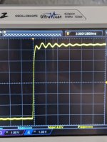
The source of the oscillation has been found, and fixed. Attached is the square wave response, looking absolutely gorgeous.
jxdking, your suggestion about a signal showing up at the input node and the LTP CCS being unstable was completely on point.
mjona, first I tried your suggestion about reducing the LTP current, went from 140 R to 220 R for R5. To no avail, this did not stop oscillation, maybe decreased it.
Then I thought to myself, what the hell, I remember natawa saying just for safety I should change R13, the base stopper for Q7, from it's value of 1.2k to something more conservative, like 10, or 22.
So, my next step was to carry out just this. I went from 1.2k to 22, hooked up the supplies, put the scopes on, and while viewing the o-scope with NO LOAD, all I could see was noise. What an amazing feeling. I put the function generator back on and tried the square wave. Looks amazing, thanks for all of your guys' help. Really something special, thank you. Looking forward to building the second channel up, with all the modifications:
- 220 R + speedup cap in between driver emitters
- base stoppers to 2.2 instead of 22
- base stopper of CCS from 1.2k to 22
- degeneration of Q12 to 4.4k from 2.2k
- degenerate Q14 with 22 R
Again, thank you all so much, the help is so appreciated.
EDIT: Attached is another picture with 8 ohm load and higher amplitude of square wave.
EDIT2: Attached is what happens when I try to do a max power test haha. Gotta put it on heatsink. Actually, just took a look at it, the dummy load is busted haha, reads 11 ohms now crap.
I am here bearing good news.
The source of the oscillation has been found, and fixed. Attached is the square wave response, looking absolutely gorgeous.
jxdking, your suggestion about a signal showing up at the input node and the LTP CCS being unstable was completely on point.
mjona, first I tried your suggestion about reducing the LTP current, went from 140 R to 220 R for R5. To no avail, this did not stop oscillation, maybe decreased it.
Then I thought to myself, what the hell, I remember natawa saying just for safety I should change R13, the base stopper for Q7, from it's value of 1.2k to something more conservative, like 10, or 22.
So, my next step was to carry out just this. I went from 1.2k to 22, hooked up the supplies, put the scopes on, and while viewing the o-scope with NO LOAD, all I could see was noise. What an amazing feeling. I put the function generator back on and tried the square wave. Looks amazing, thanks for all of your guys' help. Really something special, thank you. Looking forward to building the second channel up, with all the modifications:
- 220 R + speedup cap in between driver emitters
- base stoppers to 2.2 instead of 22
- base stopper of CCS from 1.2k to 22
- degeneration of Q12 to 4.4k from 2.2k
- degenerate Q14 with 22 R
Again, thank you all so much, the help is so appreciated.
EDIT: Attached is another picture with 8 ohm load and higher amplitude of square wave.
EDIT2: Attached is what happens when I try to do a max power test haha. Gotta put it on heatsink. Actually, just took a look at it, the dummy load is busted haha, reads 11 ohms now crap.
Attachments

Last edited:
Brothers.
I am here bearing good news.
The source of the oscillation has been found, and fixed. Attached is the square wave response, looking absolutely gorgeous.
jxdking, your suggestion about a signal showing up at the input node and the LTP CCS being unstable was completely on point.
mjona, first I tried your suggestion about reducing the LTP current, went from 140 R to 220 R for R5. To no avail, this did not stop oscillation, maybe decreased it.
Then I thought to myself, what the hell, I remember natawa saying just for safety I should change R13, the base stopper for Q7, from it's value of 1.2k to something more conservative, like 10, or 22.
So, my next step was to carry out just this. I went from 1.2k to 22, hooked up the supplies, put the scopes on, and while viewing the o-scope with NO LOAD, all I could see was noise. What an amazing feeling. I put the function generator back on and tried the square wave. Looks amazing, thanks for all of your guys' help. Really something special, thank you. Looking forward to building the second channel up, with all the modifications:
- 220 R + speedup cap in between driver emitters
- base stoppers to 2.2 instead of 22
- base stopper of CCS from 1.2k to 22
- degeneration of Q12 to 4.4k from 2.2k
- degenerate Q14 with 22 R
Again, thank you all so much, the help is so appreciated.
EDIT: Attached is another picture with 8 ohm load and higher amplitude of square wave.
EDIT2: Attached is what happens when I try to do a max power test haha. Gotta put it on heatsink. Actually, just took a look at it, the dummy load is busted haha, reads 11 ohms now crap.
Apart from the difference in amplitude the image in the second shot is little different from the one attached to post 1.
Hmm... Maybe I was a little quick to jump the gun on the celebration.Apart from the difference in amplitude the image in the second shot is little different from the one attached to post 1.
The response looks really good with no load I guess, but with the load, you're right the response still has that ringing in it. Hmm...
It is hard keeping track of suggestions when these come from multiple sources. Fault finding is a step by step process and there are a number of things that contribute to performance that may influence stability in minor ways without being a magic bullet for a major issue like instability.
So we are back to square one. sgrossklass made pertinent comments in post 6 about the CCS operating current and the type of transistors used.
He described the LTP CCS as weird.
It is a pity this point was not explored earlier because any ripple on your positive supply has free entry via Q10 emitter to base junction - all because of a mistake in placement of the stopper resistors.
As it stands Q10 is not going to drive Q7 in any linear fashion and with Q8 constituting some form of collector load on Q10 you have the structure of an common emitter amplifier where the output is inverted with respect to the input.
The purpose of C10 is to serve as a corrective bootstrap. It will do that in a conventional CCS but here it will put supply rail ripple into the base of Q7.
So how is that going to cancel the impact of ripple entering via Q10 emitter base junction.
2 m.A. CCS adaption after Jung
I have drawn an .asc file along the lines used by Jung in the AudioXpress article with amendments in September 2007 with line rejection of 140dB.
His choice was for 2SA1016 transistors (150 V types) which he rated above MPSA56 general types used by Self which have 3 times or more capacitance at Vcb=10V.
The supply rail was +18V.
The test set up involved two voltage inputs in series Vin AC of 1Vrms and +18Vdc. The CCS loading was 1R. The result is measured between 1R and earth.
Attachments
- Home
- Amplifiers
- Solid State
- Is this too much ringing?