Thanks guys,
As my experience of Chinese PCB's manufacturers, PCBWay seems the best quality. They usually use KB (King Board, Taiwan) PCB board.
Come back into the case ALLPCB, they show to me test report of PCB (Shengyi) which passed UL94V-0 standard.
Regards,
As my experience of Chinese PCB's manufacturers, PCBWay seems the best quality. They usually use KB (King Board, Taiwan) PCB board.
Come back into the case ALLPCB, they show to me test report of PCB (Shengyi) which passed UL94V-0 standard.
Regards,
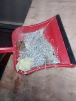
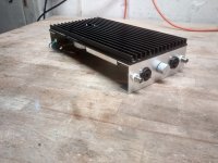
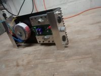
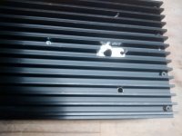
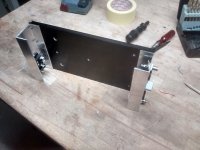
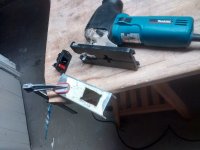
Here are some pics - metal works are finished. It looks as though there is some room for improving my free-hand routing skills.
Attachments
-
 20_scrap_IMG_20190801_205237784.jpg116.2 KB · Views: 210
 -
 19_complete_IMG_20190801_212639484_HDR.jpg193.5 KB · Views: 251
 -
 18_complete_IMG_20190801_212632675.jpg158.3 KB · Views: 238
 -
 17_xformer_IMG_20190801_202929050_HDR.jpg100.8 KB · Views: 181
 -
 16_routing_IMG_20190801_202404117.jpg145.6 KB · Views: 518
 -
 15_rear_panel_IMG_20190801_191955406_HDR.jpg173.6 KB · Views: 518
 -
 14_file_IMG_20190801_180809803_HDR.jpg105.7 KB · Views: 528
 -
 13_jigsaw_IMG_20190801_175524998_HDR.jpg152.4 KB · Views: 530
Last edited:
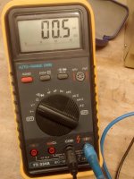
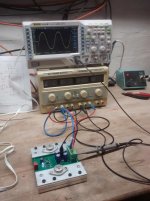
back to measurements.
Setting supply to +-30V=.
Input is shorted with a jumper.
Current consumption is close to 0.3amps.
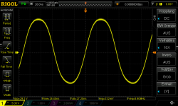
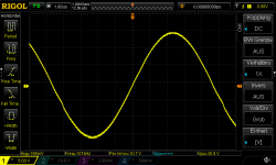
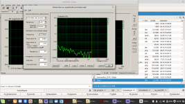
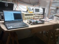
A first measurement with the scope
Setting supply to +-30V=.
Input is shorted with a jumper.
Current consumption is close to 0.3amps.
A first measurement with the scope
Attachments
Last edited:
A quick and dirty output snubber 10nF in series with 5R6 tames that beast.🙂
Total current consumption dropped to about 50mA.
Total current consumption dropped to about 50mA.
Last edited:
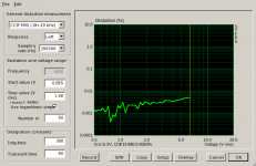
Some measurements with +-30V supply, 5R0 dummy load and sine wave input. It should be mentioned that the dummy incl wiring is not really inductorless - at 1MHz this load is neglible.
Attachments

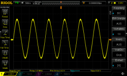
The 100kHz sine plots show some irregularities, obviously crossover distortion. Power MOSFET bias was near 30mA, so I changed the bias setting to about 80mA yielding a smoother curve shape. I guess even more bias may be advisable.
Back at audio frequencies I started distortion measurements with ARTA and my EMU 0202 USB-soundcard.
To avoid disappointments while hunting for ultra low THD results it is a good idea to examine the limits of the measurement setup first- i.e starting with a loopback measurement.
Back at audio frequencies I started distortion measurements with ARTA and my EMU 0202 USB-soundcard.
To avoid disappointments while hunting for ultra low THD results it is a good idea to examine the limits of the measurement setup first- i.e starting with a loopback measurement.
Attachments
Not too bad, but never will we measure more than two zeros behind the period with this setup.
Measuring the EUT with no load at output will show the overall residual distortion of the hole signal path - presumably dominated by the soundcard:
Measuring the EUT with no load at output will show the overall residual distortion of the hole signal path - presumably dominated by the soundcard:
Attachments
The 100kHz sine plots show some irregularities, obviously crossover distortion..
The old Hitachi lateral mosfet datasheet recommended 100mA bias current.
Anyway, distortion of this amp is in the league of my soundcard. To improve measuring resolution a bit I shall increase the amplifiers gain from 10V/V to 33V/V while trying not to change loop gain. This will relax the limited output level of the soundcard enabling operation closer to its own sweetspot.
Last edited:
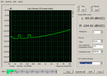
Using ARTAs level meter I measured output noise with potentiometer set to minimum i.e. input shorted.
Reading -93dBV C-weighted computes to 22uVrms output noise or 0.68uVrms input referred noise.
Until now this is the lowest noise level I measured this way with my USB soundcard setup.
Reading -93dBV C-weighted computes to 22uVrms output noise or 0.68uVrms input referred noise.
Until now this is the lowest noise level I measured this way with my USB soundcard setup.
Attachments
Last edited:
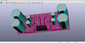
This time I ordered the pcbs at JLCPCB. Considering the non-standard dimensions of 130x50mm their offer is a really bargain.
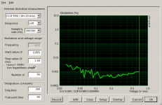
To investigate the influence of output bias setting I patched a trimpot to the bias circuit. Sweeping from 50 ~ 150mA nearly made no difference. But moving the output wires from one side to the other made a visible change of the level of the higher harmonics resulting in a slighty better THD number. So I guess that at the time the distortion is dominated by some parasitic coupling and thus more a matter of physical layout than of the bias setting. Here we have asymmetric input and output - generally not the best prerequisites for ultra high S/N. This is where theory (LTspice) meets the real world.😀
Nonetheless I will present current THD measurement at 1kHz, 10Vrms into 5 Ohms.
You can see the harmonic levels:
H1 -17.6dBFS
H2 -118dBFS
H3 -135dBFS
Nonetheless I will present current THD measurement at 1kHz, 10Vrms into 5 Ohms.
You can see the harmonic levels:
H1 -17.6dBFS
H2 -118dBFS
H3 -135dBFS
Attachments

Last edited:
Obviously measuring harmonics with amplitudes approx 100dB below the signal is not an easy task. So I have an idea for an alternative approach: Instead of measuring the output at the sources of the FET let us measure their gate voltage. Here the hole crossover distortion of the output devices is available, several orders of magnitude higher than at the output (greetings from the Quad amp). I suspect that setting the bias to minimal THD at the gates should minimize crossover distortion as well - at least theoretical. And as we all know, the difference between theory and reality is - theoretically - none!
Last edited:
- Home
- Amplifiers
- Solid State
- Just another lateral FET amp