Krisfr, the DMMT devices are duals and these indicate thermal coupling, not vbe matching. The goal of the exercise was to produce a general purpose solution that does not need tight vbe or thermal matching. The duals were a suggestion because they are availabe at low cost. The input transistor and transistor as diode operate at the same voltage and current, resulting in thermal tracking if they are in the same area. Build the version you prefer. If drafting of the PCB accommodates singles or duals, that is simply a bonus.
Documentation is being prepared that aggregates both versions of the design and will provide information for build options. This should be available by the weekend.
Thank you for being polite. 'Mr' is not required, Spladski is just fine. We are all friends here, even if discussion at times becomes contentious.
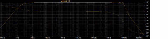
daodad, I'm uncertain how to interpret your AC analysis plot. Does it indicate that the amplifier's open loop gain bandwidth product is (5.27E6 * ClosedLoopGain)? And therefore the closed loop bandwidth is 5.3 MHz? That's quite a bit higher than the closed loop bandwidths in, for example, Bob Cordell's book. Those mostly have OLGBWP of approx 10 MHz and a closed loop bandwidth of approx 0.5 MHz.
This is Loop Gain plot (Open Loop minus Close Loop), and 5.27 MHz is ULGF.
So, closed loop bandwidth is 5.27 MHz. 10X higher than the closed loop bandwidths of the relatively blameless amps in Cordell's book.
Spladski In order to avoid contentiousness, I thought it would be nice to say Mr. 😀. When I can use LTSpice like the pros here, I will be more comfortable. I will look forward to the weekend info and share some of what I have done on the board. Some more input as to the connectors would be nice, but I will go with what I have otherwise. Some input on using Ostripper's Class H power design would be great too. It would be added as an option if there are no ethical objections. He put a great deal of work in developing that topology. I will be doing at first 2 boards for the front IP area. One for each schematic. One question, I am assuming that the servo 3 op amps go on the IP board, please correct me if I am wrong. They take a lot of the board space, and I am wondering about the power for them too.😕Documentation is being prepared that aggregates both versions of the design and will provide information for build options. This should be available by the weekend. Thank you for being polite. 'Mr' is not required, Spladski is just fine. We are all friends here, even if discussion at times becomes contentious.
So, closed loop bandwidth is 5.27 MHz.
Nope, it's ULGF divided by the closed loop gain (in a single pole approximation). ULGF equals the closed loop bandwidth only at unity gain.
Krisfr, about the ICs, I think there is no need for an electrolytic capacitance near the rails. Better a small tantalum or ceramic. It is just for decoupling.IP COMING UP
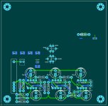
Just some idea of size and basics. The servo parts are just place holders. Actual size and dimensions will vary accordingly.😀
I'm on the exploration of the cross matched solution with your dual devices (They are supposed to be VBE matched @2mV.)Krisfr, the DMMT devices are duals and these indicate thermal coupling, not vbe matching. The goal of the exercise was to produce a general purpose solution that does not need tight vbe or thermal matching. The duals were a suggestion because they are availabe at low cost. The input transistor and transistor as diode operate at the same voltage and current, resulting in thermal tracking if they are in the same area. Build the version you prefer. If drafting of the PCB accommodates singles or duals, that is simply a bonus.
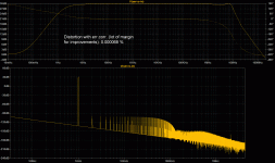
I face a strange problem of distortion, but the bandwidth and the stability margins are a lot improved. The currents are tight close, even @ 2mV mismatch, and it works perfectly with no emitter degenerative resistance.
About gain margin, my goal is always 12dB, as it is the best compromize between stability and speed.
Here what I get:
Mr spladski, trying with your file, It works perfectly. More than this, it reduces the distortion of your original file.I'm on the exploration of the cross matched solution with your dual devices
0.00008% at 50V output without error correction (while you had 0.000112).
As there is no more temp variation problems to fight, no more VBE mismatch to worry, no more tuning requested, as it is absolutely elegant, as the first and second stage are now locked together, it seems the ultimate solution for the frond end, and we could chose-it as the one one an unique version on the finish line. Just to refine the compensation.
Hoping, this time, to get an answer ....
Attachments

So
Q18 to Q1
Q2 to Q16
Q6 to Q17
Q19 to Q5
Tied Thermally...
Are there any others that need heat sinking or coupling?
Q18 to Q1
Q2 to Q16
Q6 to Q17
Q19 to Q5
Tied Thermally...
Are there any others that need heat sinking or coupling?
Krisfr, please, just wait a little more. We are on something that I'm sure will be definitive for the front end, an unique version as I said, and no need to tie the dual together, because they are by default ;-)
On the VAS side, may-be I was unclear.
My idea is to use, as an unique cooler a little metal vertical plate, crossing the board, on witch the four transistors could be fixed. So, you could just take care to align them. Q9, Q10 & Q13, Q14(on the V7 schematic).
Too Q11 ? but I'm not sure, this have to be verified in real world and an enclosure. I fear the amp could be over compensated. Q13 and Q14 do not need to be tied together, just cooled.
What do-you think ?
If you can tie together Q7 & Q8, why not ? But don't worry too much about this. We yet have a lot of gain in the front end plus a servo.
(Again it is OOT)
On the VAS side, may-be I was unclear.
My idea is to use, as an unique cooler a little metal vertical plate, crossing the board, on witch the four transistors could be fixed. So, you could just take care to align them. Q9, Q10 & Q13, Q14(on the V7 schematic).
Too Q11 ? but I'm not sure, this have to be verified in real world and an enclosure. I fear the amp could be over compensated. Q13 and Q14 do not need to be tied together, just cooled.
What do-you think ?
If you can tie together Q7 & Q8, why not ? But don't worry too much about this. We yet have a lot of gain in the front end plus a servo.
To answer to your questions with questions, what "original amp" are-you talking about, the 18 year old elector VFA Crescendo that was well known for its instability ?, or in other words, why all the automobile manufacturers design new models each year, while the Ford T was "complete and working well".What I would ask is: the original amp was complete and working well. What is your aim to change or improve in terms of performance? That should drive the development.
(Again it is OOT)
Here is my view of the first input stage PCB aimed at SMD although the parts can just as easily be through-hole.
The transistors are the MMBT5401 and MMBT5551 from Diodes Inc. These are not clones of the 2N5401/2N5551 as with other manufacturers. They did a good job of creating well matched complementary behavior. The design was consolidated to use just these parts since there was marginal difference using BC846/BC847 as current sources.
The temperature compensation has had further tuning. We will see in practice if it works. If this version validates then it will be of benefit to the wider community who may not like SMD or wish to use parts from their parts bin.
The PCB can be switched from the original config to the cascode version with jumper links. A BOM suggestion will follow. There will be a second input PCB that uses the matched pairs. I don't know about the connector scheme Rsavas refers to. Maybe he can provide info.
Place the Potentiometer.lib in the LTspice /lib/sub folder and the Potentiometer.asy in the LTspice /lib/sym folder of the root installation.
Attachments
Last edited:
Thanks Spladski, I will be looking for the BOM. I am gong to keep the op amps on the IPS if there is room. Your asc is excellent for preparation of the PCB. I may draw it up in SPlan as it gives a BOM as I go. Yes there should be some more input on the connectors. I have to investigate more to be sure. Thanks
Have-you both decided to not answer my questions any more and work apart ?
I'm on the way for an unique version, with promising result, if i believe to my sims
I'm on the way for an unique version, with promising result, if i believe to my sims
Last edited:
I have not seen your question, Sorry. ThanksHave-you both decided to not answer my questions any more ?
Krisfr, don't worry, it is not so much you but rather Spladski.I have not seen your question, Sorry. Thanks
I was worrying you to loose time on two versions while it seems absolutely possible to finish with one that can accommodate with several preferences.
I really need to discuss on few details of his version before to propose the united one.
One or Two, it or they can be done.
Please show were the adjustments, resistors, jumpers and test points are needed on the op amps. Will it be the same for both designs? Also the power sources for them. Thanks
Please show were the adjustments, resistors, jumpers and test points are needed on the op amps. Will it be the same for both designs? Also the power sources for them. Thanks
The only test point (will be indicated as TP on the schematic): Output of the first op amp.Please show were the adjustments, resistors, jumpers and test points are needed on the op amps. Will it be the same for both designs? Also the power sources for them. Thanks
I think we could use a dual OPA for U01 & UO3 and a single for U02. If there are several versions (but I don't see any interest anymore), yes, they gonna be the same.
The R103 will be an 1K adjustable, preferably multi turns.
The 2 positions switch (on/off) indicated on the schematic , I don't know if it should be a good idea to offer-it as an external switch for the user can chose error correction or not as a feature for he could chose what he prefers in listening ?
The return line from the servo to the amp need to be disconnected and its 1k free connection on the amp to be grounded, just the time for the user to adjust the offset, then reconnected. Jumpers here could be a good option ? From the 1K (Servo out in the amp) to ground or to the servo out (of the servo op amp.
Thanks a LOT Krisfr.
Last edited:
The return line from the servo to the amp need to be disconnected and its 1k free connection on the amp to be grounded, just the time for the user to adjust the offset, then reconnected. Jumpers here could be a good option ? From the 1K (Servo out in the amp) to ground or to the servo out (of the servo op amp.
Not needed. You can leave the servo connected during the offset adjustment. Just measure the servo output while doing the adjustment and adjust for zero servo output; that is the point where the amp offset is nulled.
Jan
The correct approach to development is to establish a baseline so that further modifications have a benchmark. It is not guaranteed that LTspice performance improvements will be realized with each modification. The first input PCB is the baseline. Others can follow.
Here is the BOM. I have included other component references since there will be a fair amount of experimentation. There is an interesting LED which has differing technologies for a combined Red/Yellow output. The forward voltage is almost the same, but the temperature coefficient is different.
The BOM is xls so just change the suffix.
Attachments
The correct approach to community development is communication.The correct approach to development is to establish a baseline so that further modifications have a benchmark.
You started with my project, but from the beginning you seem to be doing it all alone. I was listening to all your ideas. I even went so far as to use your last version for evaluating WITH YOU my last idea that was an add to one of yours, so that you could simulate it more easily and comment on it, and by diplomacy. And I seem to have always been friendly.
Your last answer is not.
Now, here we are. The version 7, renumbered, was supposed to be the base of future work. You continue with your own numbering that does not help.
(we can add all components we want by adding a letter to new added components ... before the definitive version)
Resuming your idea of using pairs of transistors from DIODE (well chosen by you, easy to find and inexpensive) and their base-emitter junctions as diodes, I continued by metricizing the two sides of the input stages. With good results. And it is elegant, beautifully symmetrical and simple. I have explained-it, and bring datas.
This offers the benefits of our two different approaches: The precision of mine and the greater tolerance of yours with its elimination of the need for adjustment by the manufacturer. Without major loss of performance, without thermal drift, without VBE divergence problems.
I was waiting for your answer in a "collaborative and friendly spirit".
As far as i'm in concern, I will not follow-you immediately on a cascoded input. It is an audio amplifier. Cascodes have a character, and I don't know if two of them in the same amplifier is not two much without to listen to it. As you don't provide datas of this last evolution of your own that enlighten a major advance, that look like a way-back to the adjustments YOU tried to eliminate up to now.
If you want to lead your own project, open your own thread, but, if you want we continue to collaborate, please, collaborate, comment others propositions and answer questions.
For everything to be clear, I join the ASC of this suggestion that, strangely, you insist to ignore.
Each pair is shared by the two stages, that balance themselves in a perfect way. Performance is very good, including bandwidth that I was able to extend up to 10MHz (with not enough gain margin). And there is a lot of margin, open to improvements, by adjusting the gain of the two stages (Input and VAS) for the best compromise and distortions.
It is just a file in progress: lot of things need to be improved, specially the compensation that have a great impact on distortions (we don't need this bandwidth) and, of course, the gain margin.
After this, we could see if major improvements could be achieved with the same pairs with a cascoded input. But, please, let-us work together, friendly, one step after an other.
Right, Jan, but, here, we have a special kind of servo.Not needed. You can leave the servo connected during the offset adjustment. Just measure the servo output while doing the adjustment and adjust for zero servo output; that is the point where the amp offset is nulled.
We need to adjust the perfect subtraction between input and output signal that eliminate most of the signal and this is used both for error correction and servo. And it can be a little tricky, when we are far from this point, with the gain of the second OPAMPs stage (saturation).
We have 3 opamps. it seems reasonable to can look at the output of each and a little test point or a two position jumper is not something difficult to provide. And it helps to diagnose in case of failure or amp offset problems. if you simulate the operation, you will see that it is easier to start to adjust first the amplifier offset all alone, before to adjust the precise subtraction balance.
Attachments
- Home
- Amplifiers
- Solid State
- Pizzicato, a 200W low distortion CFA amplifier