Are you mixing up noise per FFT bin and noise integrated over the band? The noise in post 2135 is apparently about -82 dB unweighted over the 200 Hz to 20 kHz band: the last plot shows a noise+distortion of 5.6658 % or -24.93 dB while the signal is around -57 dB, and there are no large distortion components visible, so noise should dominate. The before last plot looks better, though: -47 dB signal, -49.72 dB THD+noise -> -96.72 dB noise.
Last edited:
Just to clean up any misunderstandings, the pics I showed was 0 , -10, -20 , -30, -40, -50, -60 dB from PC.
Are you mixing up noise per FFT bin and noise integrated over the band? The noise in post 2135 is apparently about -82 dB unweighted over the 200 Hz to 20 kHz band: the last plot shows a noise+distortion of 5.6658 % or -24.93 dB while the signal is around -57 dB, and there are no large distortion components visible, so noise should dominate. The before last plot looks better, though: -47 dB signal, -49.72 dB THD+noise -> -96.72 dB noise.
Probably I am, but again, my main reason to show the graphs, was not to show noise performance, but the absent of harmonic components in the -40 to -60 dB , as this has been the biggest issue in my former measurements. The noise is for a large part from my poor measure setup.
Koldby,
Decent results for a simple solution 🙂
Your not returning to Zero, so I suspect the conversion error will take the form of white noise - maybe one of the reasons you have a high noise floor.
Whats your clock like? are you feeding your clock directly into the FF then the USB interface (so you Master clock is on the side of the FF?
Also the THD readings aer incorrect for the higher output levels, not sure whats going on there...
John,
That may be the result of *not feeding a virtual ground I-V converter.
Using 'voltage OP' mode results in modulation of logic gate's (flip flop) OP impedance.
You can see this quite clearly in DACs such as Sabre, where 'voltage mode'
has degraded distortion compared to 'current mode' using virtual ground.
It appears to be a significant contributor, as in Sabres case, each OP logic
gate, from memory feeds only a 50k resistor *and the DAC works in
balanced mode - but there is still a significant THD increase.
PS - Thanks for your previous contributions. As always, very useful and practical information.
Q - Have you ultimately achieved better results using chips or discrete DAC implementations?
T
@Marcel & JohnW: Just a brief comment (I'm underways with a PCB layout) to say that I have read your comments & seen your links and I looks forward to addressing the RTZ etc. in not too long.
Cheers,
Jesper
Cheers,
Jesper
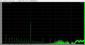
In order to be able to see more clearly the harmonics and noise and where the noise comes from, I made a x100 amp with a LME49710 and the -60 dB result can be seen in pic.1.
The harmonics are not buried in the noise here, but pretty low anyway IMHO
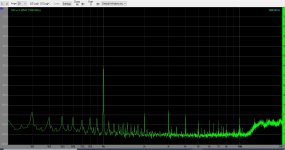
I thought the noise spectrum looked a little strange, so i looked for places where airborne noise could come from. Turned out that the inductors I was using was indeed picking up a lot of noise so I removed them and now there is only a simple R-C filter (1K- 2N2). The result in pic. 2.
NB!
The dB scale is different in pic.2. in order to see the noise floor.
Any comments?
The harmonics are not buried in the noise here, but pretty low anyway IMHO
I thought the noise spectrum looked a little strange, so i looked for places where airborne noise could come from. Turned out that the inductors I was using was indeed picking up a lot of noise so I removed them and now there is only a simple R-C filter (1K- 2N2). The result in pic. 2.
NB!
The dB scale is different in pic.2. in order to see the noise floor.
Any comments?
Attachments
Last edited:
John,
That may be the result of *not feeding a virtual ground I-V converter.
Using 'voltage OP' mode results in modulation of logic gate's (flip flop) OP impedance.
You can see this quite clearly in DACs such as Sabre, where 'voltage mode'
has degraded distortion compared to 'current mode' using virtual ground.
It appears to be a significant contributor, as in Sabres case, each OP logic
gate, from memory feeds only a 50k resistor *and the DAC works in
balanced mode - but there is still a significant THD increase.
Terry,
Its a fact of life that sadly the array resistors on the ESS DAC's suffer from "Poor" Voltage coefficient (that is there resistance value changes with voltage across them) - VC modulation is seen as ODD Order distortion products (Change of "Gain" over cycle) - as the distortion is Odd order in nature it is not cancelled by differential summing.
BTW. the ESS Element resistors are 25K... and 1/4 that value on the 9038Pro
The VC modulation of the array resistors can only effect the THD performance (it has no noticeable impact on noise).
Q - Have you ultimately achieved better results using chips or discrete DAC implementations?
At the end of the day there is no reason a Discreet DAC should measure worst then a integrated solution only the design challenges are much harder, and in fact in some cases easier (such as poorer VC of silicon resistors):-
1. Native resolution of the DAC (easier to achieve lower noise with high bit Sigma delta).
2. Clock phase (High bit Sigma delta relaxes the Clock phase noise requirements).
3. Modulator order and Pole splitting... ("shape" of the Feedback Gain).
4. PSU noise
5. DAC output impedance (thermal noise of resistors / Array).
6. PCB / Die layout
With ESS DAC's essentially the noise limitation is due to the thermal noise of the array impedance (resistance)...
I'm designing a discrete DAC with a 25 ohms output impedance - ignoring the Noise shaper libations of a 1 bit system, its the thermal noise of this 25 ohms that will limit DAC's the noise performance.
Sonicaly I prefer low order noise-shapers with NO pole splitting, this impacts the noise floor at HF but I certainly cannot hear much above 15KHz, especially below 100dB! Low order noise shapers behaved well "dynamically" - especially during large changes of state... High order Noise shapers - especially with Pole splitting are just chaotic "Dogs" - sure everything looks nice with steady state sign waves, but stimulate the system with large changes of state and the output of each Noise-shaper "Node" can be seen to go nuts with wild excursions - then taking a long time to "Settle".
I still prefer the sound of the Philips SAA7350 noise sharper with all its MANY technical "warts" to any of todays ESS DAC"s.... and there is a HUGE margin in Sound quality.
This is an example of where a State of the art measuring DAC sounds worst then a "technically" inferior measuring DAC's - steady state test signal are not good at exposing such failings.
Also, systems with multiple internal feedback paths (such as Noise shapers) are good at hiding such ills - you need to develop tests that really expose such limitations.. and its not simple THD / SNR, some of these tests can only be analysed with access to each internal node of the feedback system monitoring the internal nodes response to transient events.
What I'm trying to say is that THD / SNR is not a sonic performance matrix with complex "digital" systems...
Last edited:
Probably I am, but again, my main reason to show the graphs, was not to show noise performance, but the absent of harmonic components in the -40 to -60 dB , as this has been the biggest issue in my former measurements. The noise is for a large part from my poor measure setup.
koldby,
I'm late this this thread, (I could not visit the forum for a few years as XP users (such as myself) where no longer supported / blocked) - so I did not see your earlier attempts (with high even order distortion). However, I suspect you where not operating in balanced mode and -40dB to -60dB would be the THD I'd expect to the in a SE system due to non matched Logic output Resistances between High/ Low states.
It also shows you have good transformers.
If you look at Marcel's ADC, you can see the 02 NOR Gates after the D-type FF and “Enabled” by the Clock performing the RTZ – although I'd expect to see AND / NAND Gates here??? (I'd need to simulate Marcel's design on paper to see whats going on here) – but typically I'd Logic AND / NAND the Data with Clock to form a RTZ “Gating” effect.
I still had to come back to this...
Suppose you try to make a return-to-zero circuit using a positive-edge-triggered flip-flop and an AND gate. One input of the AND gate gets connected to the flip-flop output, the other to the clock signal that also drives the flip-flop's clock input.
After a high-to-low clock transition, the AND gate's output goes low or stays low. So far so good.
After a low-to-high clock transition, there are four possibilities:
1. The flip-flop's output is low and stays low. The AND-gate output then also stays low, like it's supposed to.
2. The flip-flop's output goes from high to low and the AND gate produces a narrow spike if it happens to be faster than the flip-flop.
3. The flip-flop's output is high and stays high, the AND gate's output goes from low to high with a delay that's only determined by the AND gate.
4. The flip-flop's output goes from low to high and the AND gate's output goes from low to high after the sum of the delays of the flip-flop and the AND gate.
Cases 2 and 4 show that there is still a dependence on the previous bit, which is precisely what you try to get rid of with a return-to-zero circuit. That is, the circuit doesn't do what it is supposed to do!
You can fix this by delaying the clock to the AND gate slightly, so the flip-flop has always settled before the AND gate sees a positive clock transition. A disadvantage is the extra jitter that the delay circuit produces, although that can be quite limited for a delay circuit with a small delay and a reasonably clean supply.
Now consider a circuit using a NOR gate connected to the flip-flop's clock and to the flip-flop's inverted output. Assuming that the difference in delays from the two NOR gate inputs is smaller than the flip-flop's delay, which will normally be the case, you get these possibilities:
Low-to-high clock transition: NOR gate output either stays low or goes low after one NOR gate delay
High-to-low clock transition:
1. When the flip-flop's inverted output is high, the NOR gate's output stays low
2. When the flip-flop's inverted output is low, the NOR gate's output makes a low-to-high transition after one NOR gate delay
That is, there is no dependence on the previous bit anymore.
True about the "Runt Pulses" due to the propagation delay of the FF - On the Dacapo Discrete DAC section I used the pair of spare NAND's in the Quad 74AC00 packaged to add the extra delay 🙂
Once my heads clear (building PCB's ATM) I'll "sim" the NOR RTZ on paper to picture what your doing - I'm not good with mental simulation of logic in my head, simple Squared paper works well for me 🙂
Once my heads clear (building PCB's ATM) I'll "sim" the NOR RTZ on paper to picture what your doing - I'm not good with mental simulation of logic in my head, simple Squared paper works well for me 🙂
Last edited:
koldby,
I'm late this this thread, (I could not visit the forum for a few years as XP users (such as myself) where no longer supported / blocked) - so I did not see your earlier attempts (with high even order distortion). However, I suspect you where not operating in balanced mode and -40dB to -60dB would be the THD I'd expect to the in a SE system due to non matched Logic output Resistances between High/ Low states.
It also shows you have good transformers.
I have actually made and measured the same circuit in balanced mode (Q and Q' as output) but with different flip flops (74HCT74 and 74AHCT74 and another fast 7474 but forgot the name) and the SE output were actually cleaner. It is only with the 74AUC1G that the results are this good. I guess that the Q and Q' are better matched and the output impedance in high and low state is better matched?
Can anybody explain to me , why the RTZ should be better? does it have better noise suppression? Does it solve more problem than it introduces?
One other thing I have been wondering about:
When I measure , I use quite high level of averaging in my spectrum analyzer (20 - 40 times) , but dosen´t this hide the random noise that comes from the circuit I measure? I imagine that it removes the noise in the measurements a little like the Signalyst DSC1 does with the actual signal?
When rise and fall times are not exactly the same, RTZ ensures that each and every 1 has exactly the same weight, independent of the bit that comes before it. Hence, it eliminates a cause of intermodulation between the signal and itself that could convert out-of-band quantization noise into the audio band. The only problem it causes is an increase in the sensitivity to jitter, but you can solve that again by making a FIRDAC.
(The plot shows that with unequal rise and fall times, a 1010 sequence has a different average value than a 1100 sequence when the rise time is 0 while the fall time is not.)
(The plot shows that with unequal rise and fall times, a 1010 sequence has a different average value than a 1100 sequence when the rise time is 0 while the fall time is not.)
Attachments

Last edited:
Thanks.When rise and fall times are not exactly the same, RTZ ensures that each and every 1 has exactly the same weight, independent of the bit that comes before it. Hence, it eliminates a cause of intermodulation between the signal and itself that could convert out-of-band quantization noise into the audio band. The only problem it causes is an increase in the sensitivity to jitter, but you can solve that again by making a FIRDAC.
(The plot shows that with unequal rise and fall times, a 1010 sequence has a different average value than a 1100 sequence when the rise time is 0 while the fall time is not.)
Excuse me for my ignorance, but the question remains. What does a RTZ circuit do to rectify the difference between left top and button integrate?. And would it not be better to ensure equal rise and fall times instead of complicating the circuit?
....
One other thing I have been wondering about:
When I measure , I use quite high level of averaging in my spectrum analyzer (20 - 40 times) , but dosen´t this hide the random noise that comes from the circuit I measure? I imagine that it removes the noise in the measurements a little like the Signalyst DSC1 does with the actual signal?
Good question - I wonder about that too - do we miss the dynamic behaviour of noise when averaging in FFTs?
Thanks.
Excuse me for my ignorance, but the question remains. What does a RTZ circuit do to rectify the difference between left top and button integrate?. And would it not be better to ensure equal rise and fall times instead of complicating the circuit?
If you can come up with a method to get exactly equal rise and fall times without complicating the circuit, make sure you apply for a patent before telling anyone!
With return to zero, the 1100 pattern changes into 10100000 and the 1010 pattern into 10001000. In both cases you have precisely two rising and two falling edges, so the average values are the same, even when the rise time is different from the fall time.
I see, thanks for the explanation.If you can come up with a method to get exactly equal rise and fall times without complicating the circuit, make sure you apply for a patent before telling anyone!
With return to zero, the 1100 pattern changes into 10100000 and the 1010 pattern into 10001000. In both cases you have precisely two rising and two falling edges, so the average values are the same, even when the rise time is different from the fall time.
Do I see it right when I conclude, that if the RTZ is a 50% duty cycle relative to normal shift between 1 and 0 (no a very good explanation. I hope you see what I mean) , the analog output level will be 50% less this way.
A clock buffer maybe? Are they not precisely enough?If you can come up with a method to get exactly equal rise and fall times without complicating the circuit, make sure you apply for a patent before telling anyone!
I think the reason the 74AUC1G is performing so well is that when operating near its VCC limit, the rise and fall times are most equal and better that the other F-F I have tried.
I see, thanks for the explanation.
Do I see it right when I conclude, that if the RTZ is a 50% duty cycle relative to normal shift between 1 and 0 (no a very good explanation. I hope you see what I mean) , the analog output level will be 50% less this way.
Yes, the idea is to RTZ for EVERY clock cycle irrespective of the input Data. In the case of a simple NOR / NAND arrangement your "Gating" your DATA pulses via the clock so you have a 50% "On" Pulse (so the results is 50% "integrated" energy from your PSU rails).
There are many other methods to generate a RTZ scheme - so a 50% pulse energy reduction is not a given - the design I'm currently working on I've reduced the RTZ "Zero" state to 1/4 of the pulse "On" period as 'm aiming for an improved SNR.
With good clocking, PSU and design I've seen 130dB+ DNR Atwd (DSD256) even with a 50% RTZ "blanking period"...
How about something like this:
https://www.idt.com/document/dst/5pb11xx-family-datasheet
For Clock distribution I just use TinyLogic Dual 04 (Inverter) / 16 (Non Inverters) as Clock buffers, I operate my array Logic at 5V - 6V for increased DNR.
If you operating with near 100MHz Clocks at 5V dont be caught out by the higher then expected power dissipation of CMOS logic.
Last edited:
- Home
- Source & Line
- Digital Line Level
- The Best DAC is no DAC