COD is large signal - agreed - but I was simply pointing out to (Herve IIRC) that low closed loop gain 'COD like' behaviour in a VFA is nothing to do with CFA COD and everything to do with a sub-optimally compensated amplifier that will oscillate.
I am not sure to understand what you say, but I repeat here that COD feature is absolutly not a problem for VFA, and this feature appears on VFA before its implementation on CFA.
The CFA trick is however that its possesses COD (large signal behaviour) which a VFA in its classic guise (LTP, MC compensated, no tricks) does not.
Single input device CFA don't have COD behaviour.
There is a graph provided in the reference, the deviation is substantial above ~2V Vce.
Yes, I see. And yet, curve traces that would seem to belie that graph are readily available.
Attachments

I am not sure to understand what you say, but I repeat here that COD feature is absolutly not a problem for VFA, and this feature appears on VFA before its implementation on CFA.
Single input device CFA don't have COD behaviour.
When you can explain, clearly, the difference between a CFA and a VFA, and stick to it without changing the facts every time to suite your interpretation of reality, I may be able to respond. Until then, we just have to agree to not agree on anything.
When you can explain, clearly, the difference between a CFA and a VFA, and stick to it without changing the facts every time to suite your interpretation of reality, I may be able to respond. Until then, we just have to agree to not agree on anything.
Andrew,
I wrote many time what are the differences between VFA and CFA and never change the facts.
I posted simulation of most of my statement so you can't say I interpret reality.
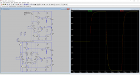
Look at the attachement. I only add a diamond to a CFA. Of course the scheme are not optimal as I drew them in 2'. But it is easy to see that the VFA has the COD feature, and by changing R26 I can have constant bandwidth as with a CFA. This is neither interpretation of reality nor fact changing.
Attachments
Single input device CFA don't have COD behaviour.
Sorry, it does. It is though difficult to compare a single input CFA with a VFA, since you can't always consistently implement Miller compensation. But an (otherwise suboptimal) shunt compensation in a sigle ended CFA will show the COD effect.
Last edited:
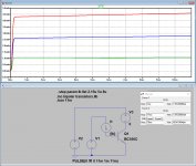
Thevenin translation
Below is a Thevenin translation of a simplistic Rf - Rg feedback network. This represents the foundation of the thought process behind several arguments presented in the past.
It is considered that much of the difficulty in comprehending the nature of a CFA results from the elusive relationship that the In- terminal has to an elusive voltage that must exist to support the functionality of the device. The Thevenin translation is intended to identify that elusive potential as V Thevenin.
Using the Thevenin translation it can easily determine the value of Vin necessary from selecting an arbitrary Vout, and specifying resistances at the Tz node and for Rf and Rg. These Vout and Vin values can then be applied to the simplistic non-translated Rf - Rg network to verify the summation of currents at the In- terminal and their current phase relationship.
Before presenting any further arguments, does anyone consider such translation as potentially useful to simplify their the understanding of a CFA.
Attachments

Yes, I see. And yet, curve traces that would seem to belie that graph are readily available.
This needs more study, there are multiple issues in looking at this in all detail. Characteristic curves can be vs. Vbe or Ib, since beta can be a strong function of Ib I personally find this approach (bipolars as current controlled devices) virtually useless. My last product with patent was a constant BW log amp where the log conformance of a tiny short base NPN was quite good from 100fA to 100uA (collector current).
Sorry, it does. It is though difficult to compare a single input CFA with a VFA, since you can't always consistently implement Miller compensation. But an (otherwise suboptimal) shunt compensation in a sigle ended CFA will show the COD effect.
I think I demonstrated the contrary in post #2056.
I implement a large shunt capacitor to show the effect.
Can you tell me what is wrong ?
I would be surprised if the current LTSpice models would be so wrong.Ian, thanks for looking into this. The results are worrisome for our general use of LTSpice.
Regardless of the transistor spice models we use, the Ebers-Moll/Early equations and the Hybrid Pi model support the existence of the small signal effect I was discussing. It would surprise me if the non-ideality of these were so extreme as to make the effect itself questionable, but what appear to be the relevant issues are the values of various parameters and the extent to which the effect occurs.
In CPaul's CFA circuit I replaced the Cordell modelled BC550 and BC560 with transistors having no Ro at all.
Placing 230K resistors in parallel to these transistors gave me exactly the same result as the BC550/BC560.
An Ro of 230K is a very realistic value at 1mA for these transistors, so if the VBIC model has 10 times less variation in this situation, it would mean a very unrealistic Ro of 2.3Meg.
Hans
I think I demonstrated the contrary in post #2056.
I implement a large shunt capacitor to show the effect.
Can you tell me what is wrong ?
The current provided by the feedback resistor is too small, and the shunt cap is to large to clearly reveal the COD effect. Try something based on CCVS and VCVS and you should see it clearly, once you are free of the bias constraints.
TNT,
We can only mitigate the disease by thoughtfully choosing (discrete) devices, topology and biasing scheme. The less op-amp features the better.
Hierfi,
regarding post #1747
Unlike in mathematics, in the physical world everything always occurs at the expense of something else. Achieving high unloaded single transistor amplifier bandwidth is trivial, providing adequate stable static (DC bias) bandwidth and maintaining a wide dynamic range is not. (Frequency is inversely related to current and amplitude).
Industrial applications have their own objectives, need not worry about audio signal distortion. Borrowing ideas, circuit solutions and part selection strategy from those sources may be short-sighted and counterproductive.
The interelectrode capacitances constitute the transistor thus are not parasitic but essential. They cannot be "nullified or eliminated", however, measures aiming to prevent excessive proliferation can be taken - at the cost of amplification factor and efficiency.
I am struggling to interpret your arguments in general.
Happy New Year to everyone!
N101N, can you name an amp that does not suffer from the illness you describe?
We can only mitigate the disease by thoughtfully choosing (discrete) devices, topology and biasing scheme. The less op-amp features the better.
Hierfi,
regarding post #1747
Unlike in mathematics, in the physical world everything always occurs at the expense of something else. Achieving high unloaded single transistor amplifier bandwidth is trivial, providing adequate stable static (DC bias) bandwidth and maintaining a wide dynamic range is not. (Frequency is inversely related to current and amplitude).
Industrial applications have their own objectives, need not worry about audio signal distortion. Borrowing ideas, circuit solutions and part selection strategy from those sources may be short-sighted and counterproductive.
The interelectrode capacitances constitute the transistor thus are not parasitic but essential. They cannot be "nullified or eliminated", however, measures aiming to prevent excessive proliferation can be taken - at the cost of amplification factor and efficiency.
I am struggling to interpret your arguments in general.
Happy New Year to everyone!
My last product with patent was a constant BW log amp where the log conformance of a tiny short base NPN was quite good from 100fA to 100uA (collector current).
Great, that's a whopping 180 dB range. What's the BW and deviation from the log function? IC on the way already?
The current provided by the feedback resistor is too small, and the shunt cap is to large to clearly reveal the COD effect. Try something based on CCVS and VCVS and you should see it clearly, once you are free of the bias constraints.
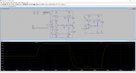
Attached is the respons of a single input device CFA and a Diamond CFA, in the same conditions.
It is clear that Diamond CFA shows COD effect and single input device doesn't. It works on one polarity, on the other one slew rate is limited by the transistors bias currents.
Attachments
On the single ended I’d say you have COD in operation in the positive going direction. In the negative going direction, the 4n7 cap can only be discharged by the current source U5 so the fall time is much longer.
To check the effect, you need to look at the current flowing in Re.
To check the effect, you need to look at the current flowing in Re.
On the single ended I’d say you have COD in operation in the positive going direction. In the negative going direction, the 4n7 cap can only be discharged by the current source U5 so the fall time is much longer.
Agreed !
As the diamond topology controls the 2 currents polarities, it has COD effect. COD is a property of diamond or assimilated but not a CFA property.
Agreed !
As the diamond topology controls the 2 currents polarities, it has COD effect. COD is a property of diamond or assimilated but not a CFA property.
This boils down again to the CFA definition. I see a chicken and an egg here. I thought it was already agreed that CFAs are nothing more than a particular clever circuit topology?
Not sure what was your expectation here, symmetrical slewing property from an asymmetrical CFA? Try getting symmetrical slewing from a Linn topology VFA.
I think the problem is that when I write :
"Single input device CFA don't have COD behaviour."
Your reply is :
"But an (otherwise suboptimal) shunt compensation in a sigle ended CFA will show the COD effect. "
So instead of giving your very good advices on symetrical slewing, try to read slowly.

I did the Early Effect Sim for the BC550C.Yes, I see. And yet, curve traces that would seem to belie that graph are readily available.
The horizontal scale from 0 to 11 msec should be read as Vce from 0 to 11 Volt.
The difference between 1volt and 11Volt at Ic = 1mA is 60.4uA.
This gives a value for Ro of 10/60.4e-6 = 165K, which seems perfectly O.K.
Doing the same with the BC560C resulted in 170K for Ro.
So the early effect is well showing up, exactly as expected and with realistic values.
I see no reason to change to VBIC.
Hans
Attachments
Below is a Thevenin translation of a simplistic Rf - Rg feedback network. This represents the foundation of the thought process behind several arguments presented in the past.
It is considered that much of the difficulty in comprehending the nature of a CFA results from the elusive relationship that the In- terminal has to an elusive voltage that must exist to support the functionality of the device. The Thevenin translation is intended to identify that elusive potential as V Thevenin.
Using the Thevenin translation it can easily determine the value of Vin necessary from selecting an arbitrary Vout, and specifying resistances at the Tz node and for Rf and Rg. These Vout and Vin values can then be applied to the simplistic non-translated Rf - Rg network to verify the summation of currents at the In- terminal and their current phase relationship.
Before presenting any further arguments, does anyone consider such translation as potentially useful to simplify their the understanding of a CFA.
I have considered making the very same argument. The input stage does not experience a difference between the two circuits. And now, we no longer have to deal with the argument that the input stage current flows only through Rg. Now the input stage current flows from the "new" output, Vth.
But the same current flowing from the output through the input stage will, I fear, still be ignored in favor of the observation that the transconductive portion of the input transistor current is a function of by vb - ve. For a few folks, for some reason, this excludes the possibility of any kind of feedback of any current. It is this assertion that needs to be at the forefront of further discussion between the two camps. But perhaps Hierfi's Thevenin equivalence will move us closer.
- Home
- Amplifiers
- Solid State
- Current Feedback Amplifiers, not only a semantic problem?