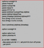
If someone nedds the asc, here it is. Note that the driver Transistors are 2N2222 from the LTSpice 4 stock lib. Replace it with your own Modell.
Thanks, appreciate that. 😉
Norman.
needs some action, isn't it?... I think its a lot of latent potential!
The circuit looks picture perfect as far as symmetry is concerned. What has escaped people's notice is in any quasi-complementary output stage you will never see an emitter resistor in the lower NPN power transistor connection to the negative supply - R18 in John's circuit.
Many think current travels from the collector to the emitter of a transistor but this is a notional thing as the charge carriers, electrons in the case of an NPN device, run in the reverse direction.
With a 0.5 Ohm resistor passing 2A there is a negative feedback voltage of 1 at the emitter. This will reduce the base-to-emitter voltage - with limiting flow on implications.
Measured against Linsley-Hood's 1996 Class A circuit with a standing output stage current of 2A with a peak capacity of 3.3A shows a short fall - to offset the difference placing R18 between collector and the output rail would raise the output Iq.
Some resistor values may need to change depending on the desired Iq level. This would have other impacts on the circuit. I looked for possibilities which could be used to advantage. In the end the dominant pole requires only one capacitor.
I have THD and Tian probe simulations - contact me if you want the details.
Can this circuit work in AB mode with high bias? If we keep the bias at say 800ma , can it give up to 10 watts in class A and then slide nicely into class B? How bad are the Distortion products in class B?
Can this circuit work in AB mode with high bias? If we keep the bias at say 800ma , can it give up to 10 watts in class A and then slide nicely into class B? How bad are the Distortion products in class B?
That is an interesting thought but you would need a different output stage.
Thanks mjona, for your comments...
like i said before, i think circuit holds potential, only needs fine tuning by experts.
I am none in this regard...
Prasi
like i said before, i think circuit holds potential, only needs fine tuning by experts.
I am none in this regard...
Prasi
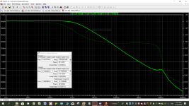
I can't quite tell how to interpret the frequency response plot in post #33.
It appears that the "gain" curve crosses below 0dB at 10 MHz; I hope I have that right.
Is "10 MHz" the raw amplifier circuit's open loop bandwidth from input to output, when the feedback divider network (R6-R4) is omitted?
Or is "10 MHz" the bandwidth of the amplifier AND feedback divider network (R6-R4), all around the loop? If so then the raw amplifier all by itself would have an open loop bandwidth 15.7X higher, namely 157 megahertz. That would be a remarkable achievement using 2N3055 devices.
(R6+R4)/R4 = 15.7
mjona- the purpose of the emitter resistor in the lower 2N3055 emitter is to provide local NFB. In this circuit, as in the JLH, current can only swap between the upper and lower devices to drive the output in push-pull. As has been pointed out in the JLH 10W thread, the current increase in one device can only come from a decrease in current in the other. In the original JLH, a gain reduction in the transistor with increasing current limits the output current unless there is an increase in Iq. Using emitter resistors provides greater symmetry between the upper and lower devices though the (slight) increase in local NFB.
- Mark J I cannot check the data at present. mjona might be kind enough to publish his Tian plot.
- Mark J I cannot check the data at present. mjona might be kind enough to publish his Tian plot.
Last edited:
I can't quite tell how to interpret the frequency response plot in post #33.
It appears that the "gain" curve crosses below 0dB at 10 MHz; I hope I have that right.
Is "10 MHz" the raw amplifier circuit's open loop bandwidth from input to output, when the feedback divider network (R6-R4) is omitted?
Or is "10 MHz" the bandwidth of the amplifier AND feedback divider network (R6-R4), all around the loop? If so then the raw amplifier all by itself would have an open loop bandwidth 15.7X higher, namely 157 megahertz. That would be a remarkable achievement using 2N3055 devices.
(R6+R4)/R4 = 15.7
Would you mind checking my Tian Probe settings I am getting more extreme results than these - see attachments. The Tian Probe is with the to earth decoupling open circuit. The blip at the bottom is not present with the latter closed. My feedback resistor values are 12k and 270R. There are some departures from John Ellis circuit in mine.
Attachments
gannaji
It would not work as an AB design. As explained in the above post the quiescent current in the VAS sets the quiescent current in the output which swings from 2 to 0x the standing current in each transistor (in theory). There would not be enough current to increase this beyond the doubling of the driver/VAS stages, so a different design would be needed for any swing into Class B.
It would not work as an AB design. As explained in the above post the quiescent current in the VAS sets the quiescent current in the output which swings from 2 to 0x the standing current in each transistor (in theory). There would not be enough current to increase this beyond the doubling of the driver/VAS stages, so a different design would be needed for any swing into Class B.
Last edited:
Tian Plot for your early 16A circuit.
The Tian plot of your circuit that I did had 4.7R stopper resistors in the bases of the BD139 transistors and 100p capacitors from collector to base. These were absent in the circuit in post 1 - I don't remember the how or why we can leave that for Mark J to look into. I did add a 0.22R to buffer the output where you might have used a coil.
The point at which the gain line crosses -180 degrees with both feedback elements in place is 30.96MHz.
- Mark J I cannot check the data at present. mjona might be kind enough to publish his Tian plot.
The Tian plot of your circuit that I did had 4.7R stopper resistors in the bases of the BD139 transistors and 100p capacitors from collector to base. These were absent in the circuit in post 1 - I don't remember the how or why we can leave that for Mark J to look into. I did add a 0.22R to buffer the output where you might have used a coil.
The point at which the gain line crosses -180 degrees with both feedback elements in place is 30.96MHz.
Attachments
I think you're fooling yourself quite dramatically. 160 MHz or now 486 MHz (31 MHz x 15.7) is simply not possible with a one-layer PCB using thru hole components which include the 2N3055.
Luckily you can measure the real-world bandwidth of the real amplifier sitting on your lab bench, quite easily. All you need to do is apply a fast risetime square wave and then measure the amplifier's output risetime. For single pole systems such as your amplifier, the Bandwidth - Risetime equivalency formula readily yields the desired result:
As long as you apply an input square wave with a (10% to 90%) risetime of 5 nanoseconds or less, you'll get a trustworthy measurement of your amplifier's bandwidth. Not a simulation of its bandwidth, a measurement.
The measurement gives the closed loop bandwidth of the entire amplifier PCB, including feedback resistors, operating at a gain of 15.7X. Then we simply multiply by 15.7 to find the gain bandwidth product of the raw amplifier all by itself.
I recommend using an output amplitude of about 2 to 4 volts between min and max. Enough to get a decent swing but far, far away from clipping or slew rate limiting. At your amp's gain of 15.7X that's a square wave input amplitude of about 250 millivolts.
Wikipedia thoroughly discusses, and mathematically derives, the Risetime - Bandwidth equivalency here. Derivations and thorough discussions also appear in the old, pre-uA741 textbooks, such as the ones by Middlebrook, Choma, Searle, the AARL, and so on.
By the way if you want to "cheat" or "game the system", fiddle around with the output load while measuring risetime. You'll discover that the minimum risetime occurs at an Rload value which is NOT infinity: some load is better than no load. You'll also discover that the minimum risetime needs an Rload value greater than 4 ohms. At least that's my prediction.
Luckily you can measure the real-world bandwidth of the real amplifier sitting on your lab bench, quite easily. All you need to do is apply a fast risetime square wave and then measure the amplifier's output risetime. For single pole systems such as your amplifier, the Bandwidth - Risetime equivalency formula readily yields the desired result:
- Bandwidth (in Hz) = 0.35 / (Rise time (in seconds))
As long as you apply an input square wave with a (10% to 90%) risetime of 5 nanoseconds or less, you'll get a trustworthy measurement of your amplifier's bandwidth. Not a simulation of its bandwidth, a measurement.
The measurement gives the closed loop bandwidth of the entire amplifier PCB, including feedback resistors, operating at a gain of 15.7X. Then we simply multiply by 15.7 to find the gain bandwidth product of the raw amplifier all by itself.
I recommend using an output amplitude of about 2 to 4 volts between min and max. Enough to get a decent swing but far, far away from clipping or slew rate limiting. At your amp's gain of 15.7X that's a square wave input amplitude of about 250 millivolts.
Wikipedia thoroughly discusses, and mathematically derives, the Risetime - Bandwidth equivalency here. Derivations and thorough discussions also appear in the old, pre-uA741 textbooks, such as the ones by Middlebrook, Choma, Searle, the AARL, and so on.
By the way if you want to "cheat" or "game the system", fiddle around with the output load while measuring risetime. You'll discover that the minimum risetime occurs at an Rload value which is NOT infinity: some load is better than no load. You'll also discover that the minimum risetime needs an Rload value greater than 4 ohms. At least that's my prediction.
...in any quasi-complementary output stage you will never see an emitter resistor in the lower NPN power transistor connection to the negative supply...
Attachments
I think you're fooling yourself quite dramatically. 160 MHz or now 486 MHz (31 MHz x 15.7) is simply not possible with a one-layer PCB using thru hole components which include the 2N3055.
Luckily you can measure the real-world bandwidth of the real amplifier sitting on your lab bench, quite easily. All you need to do is apply a fast risetime square wave and then measure the amplifier's output risetime. For single pole systems such as your amplifier, the Bandwidth - Risetime equivalency formula readily yields the desired result:
- Bandwidth (in Hz) = 0.35 / (Rise time (in seconds))
As long as you apply an input square wave with a (10% to 90%) risetime of 5 nanoseconds or less, you'll get a trustworthy measurement of your amplifier's bandwidth. Not a simulation of its bandwidth, a measurement.
The measurement gives the closed loop bandwidth of the entire amplifier PCB, including feedback resistors, operating at a gain of 15.7X. Then we simply multiply by 15.7 to find the gain bandwidth product of the raw amplifier all by itself.
I recommend using an output amplitude of about 2 to 4 volts between min and max. Enough to get a decent swing but far, far away from clipping or slew rate limiting. At your amp's gain of 15.7X that's a square wave input amplitude of about 250 millivolts.
Wikipedia thoroughly discusses, and mathematically derives, the Risetime - Bandwidth equivalency here. Derivations and thorough discussions also appear in the old, pre-uA741 textbooks, such as the ones by Middlebrook, Choma, Searle, the AARL, and so on.
By the way if you want to "cheat" or "game the system", fiddle around with the output load while measuring risetime. You'll discover that the minimum risetime occurs at an Rload value which is NOT infinity: some load is better than no load. You'll also discover that the minimum risetime needs an Rload value greater than 4 ohms. At least that's my prediction.
Thanks for pointing this out Mark - looking at the Tian probe test I downloaded, the outputs were MOSFET's and the probe feed is into the voltage gain stages with an assumption the MOSFET gain and phase will hold up.
The figures of 10MHz have to relate to the voltage stages whereas the unity gain of 2N3055's is around 2-3MHz so the Tian probe in it's present form is of no use. I wonder how many others who borrowed this test for similar purposes have fallen into this trap.
It may be that like the original JLH circuit the outputs being the slowest devices can be used to set the dominant pole. I have no plans to build this however if I was I would think about compensating the input LTP.
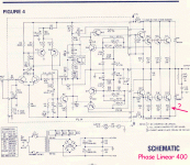
Phase Linear 400
I concede to your point however there are three power devices in parallel and the 0.22R emitter resistors are to share the load evenly. There is also a 0.22R resistor in common to the collectors of all of these R41 so you have 0.073R versus 0.22R which is more dominant.
I concede to your point however there are three power devices in parallel and the 0.22R emitter resistors are to share the load evenly. There is also a 0.22R resistor in common to the collectors of all of these R41 so you have 0.073R versus 0.22R which is more dominant.
Is the phase Linear400 is also a JLH ? How about 1001 other asymmetric (same type transistors) ones ?
Is the phase Linear400 is also a JLH ? How about 1001 other asymmetric (same type transistors) ones ?
That is or was a high power amplifier by a US maker from the early 70's - it was a leader in the power stakes competition going on at the time.
😀The plot mjona showed a UGF of about 1MHz for the loop gain. I'm not sure why the plot I generated showed 10MHz, I agree this looks wrong. I'll look into this as soon as I can.
I'm not sure now whether mjona's plot is the same circuit or not, but 1MHz is more reasonable. I certainly would not claim anything like 100MHz+ for a 2N3055 (unless perhaps the input power was greater than the output and fed straight trhough with losses 😀 )...
I'm not sure now whether mjona's plot is the same circuit or not, but 1MHz is more reasonable. I certainly would not claim anything like 100MHz+ for a 2N3055 (unless perhaps the input power was greater than the output and fed straight trhough with losses 😀 )...
Last edited:
Another SPICE tack
How about a 50kHz square wave test from Bob Cordell's SPICE tutorials. I have adapted this simulation for John's 2N3055 circuit - note the small adjustment to set the output rail at half the deflection for +/- 4 volt swings.
There is a some evidence of instability arising on negative swings. I don't know how significant this is however if as I suggested in an earlier post R18 is moved so it connects between the output rail and Q10 collector the problem disappears.
Attachments
- Home
- Amplifiers
- Solid State
- 16W Class A - inspired by JLH