Hi Ian,
All your links when clicked lead to Keith Snooks' home page. But looking at your post, the URLs are different. What's going on here, is it an issue with Keith's site?
Jan
Try this link to the December 1989 issue of Wireless World:
https://www.americanradiohistory.com/Archive-Wireless-World/80s/Wireless-World-1989-12.pdf
Note that the American Radio History website is a superb resource for old magazines. Highly recommended.
Yes, I know this resource, thanks to point out Linsley-Hoods analysis.
BTW I also read the article about that 'old' Voyager spacecraft, this was 1989, and Voyager is still en route I believe! Incredible!
Jan
BTW I also read the article about that 'old' Voyager spacecraft, this was 1989, and Voyager is still en route I believe! Incredible!
Jan
I don't think I am ignoring anything.You completely ignore the fact that there are things connected to the "bridge" at other points than only nodes A and B. If both the output of the class-A amplifier and the dumper were connected at node A or node B, I would agree, but they are not.
Hence, this statement is also wrong.
The only other connection I see is the output of the transconductance amp.
Again, the impedance seen between the output of the amp (node B) and the virtual ground is not affected by anything but the four bridge components (which equals about 500 ohms up to 1MHz) provided the bridge is balanced. Thus this path can simply be replaced by a resistor that is outside of the bridge and node A can be grounded. IOW a bridge is not required to "null out" the Vbe errors from the feedback because the feedback does not have to go via a bridge at all, which means the bridge and the need to balance it are unnecessary.
Last edited:
It is hard to check you figures but I think your gist is right. The thing I would like you to contemplate is why there is a need to balance away the Vbes of the "dumpers" at all.If you forget for the moment that there are people who call it a bridge, do you see any flaw in my calculation?
In a normal NFB topology, the feedback is sensed at the output (node B). What voltages go on at the transistor bases are not sensed. With a transconductance amplifier driving the bases the thing would operate pretty well except that there would be very fast voltage swings at the bases as the output current changes phase. Equivalent components to the Quad could be used to mitigate this.
In the Quad current dumper topology, feedback is sensed at two places neither of which is the output! One is the bases and the other is the emitters. Because of this, the Vbe voltages are sensed too. The stated aim of putting the transistors inside a balanced bridge is to try to remove the Vbe from the feedback path...the Vbe that didn't need to be in the path in the first place. Why didn't they sense the feedback at the output and avoid adding this distortion? 😕
There is a very good marketing reason for sure but I hope there is a compelling technical reason too.
TB the problem that's been pointed out to you is that your jump from figure 1 to figure 2 throws out half the circuit. Either you're going to need to show that they're equivalent or revise your analysis. At this point you've done the hand wavy engineery thing as I warned but not actually doing the engineering. And making up a new bridge circuit (fig 2) whole cloth to prove the point you want to make rather than what's actually going on.
It is hard to check you figures but I think your gist is right. The thing I would like you to contemplate is why there is a need to balance away the Vbes of the "dumpers" at all.
In a normal NFB topology, the feedback is sensed at the output (node B). What voltages go on at the transistor bases are not sensed. With a transconductance amplifier driving the bases the thing would operate pretty well except that there would be very fast voltage swings at the bases as the output current changes phase. Equivalent components to the Quad could be used to mitigate this.
In the Quad current dumper topology, feedback is sensed at two places neither of which is the output! One is the bases and the other is the emitters. Because of this, the Vbe voltages are sensed too. The stated aim of putting the transistors inside a balanced bridge is to try to remove the Vbe from the feedback path...the Vbe that didn't need to be in the path in the first place. Why didn't they sense the feedback at the output and avoid adding this distortion? 😕
There is a very good marketing reason for sure but I hope there is a compelling technical reason too.
It seems to me that we are making progress. If I understand your post correctly, you don't deny that the distortion of the dumpers is (largely) cancelled, you just wonder whether there isn't a more straightforward way to get rid of their distortion.
There certainly is in my oversimplified model, but that's due to it being oversimplified. I implicitly assumed the class-A part to have nullor properties: infinite voltage, current, transadmittance and transimpedance gain and no clipping limits. If it really had those properties, you wouldn't need the dumpers at all, you could just put a feedback loop around the class-A part and be done with it.
Slightly less theoretical but still quite unrealistic, when the class-A part has a finite transconductance but infinite output impedance and the dumpers have no collector-base capacitance (assuming they are simple emitter followers), you could just connect the class-A part to the dumpers, put a feedback loop around the combination and that's it. I think this is what you are suggesting to do.
The problem is that in reality the class-A part will have a large but finite voltage gain, so you get a dead zone, a range of input voltages where the feedback loopgain (practically) drops to zero and the amplifier (practically) doesn't react to the input at all. For example, when the voltage gain is 100 000 and the dumper transistors need 700 mV to start conducting, input voltages up to 7 uV will not result in any output. In real life the gain of the class-A part drops with frequency, so this issue will get more severe with increasing frequency.
You can mitigate this to some extent with a resistor bypassing the base-emitter junction of the dumpers, making an extra path from the class-A amplifier straight to the output. At least the loopgain then drops to a non-zero value when the signal is too small to make the dumpers conduct. This works, but you still have a very nonlinear thing inside your feedback loop and only have the loopgain to correct for its distortion. Especially at high frequencies, where loopgain drops, it will be difficult to get a reasonably low distortion out of it.
The nice thing about Quad's current dumping is that the gain of the class-A part is allowed and even supposed to drop with frequency. Otherwise it can't balance out the path through the inductor, which also drops with frequency.
At low frequencies, where the inductor is essentially a short circuit and the 120 pF capacitor an open branch, your Fig. Q1 is simply a feedback amplifier with class-C output stage having a 47 ohm bypass resistor between base and emitter of the transistors of the class-C stage.
At higher frequencies, the gain of the class-A part drops. In a normal feedback amplifier with class-C output stage having a 47 ohm bypass resistor between base and emitter of the transistors of the class-C stage, the gain drop would 1:1 result in a distortion increase. In Quad's version the distortion increase is much reduced, because the trick with the extra inductor ensures that the class-C stage's distortion is still cancelled out.
Bad links
Sorry, they work on my old PC but not on a newer PC with Win10/Chrome. A mystery😱.
Try the American Radio History site. The Moir article is "Valves versus transistors" July 1978 here (p57 of the PDF).
The Quad 405 article is here (p48 of the PDF). I hope that works.
Hi Ian,
All your links when clicked lead to Keith Snooks' home page. But looking at your post, the URLs are different. What's going on here, is it an issue with Keith's site?
Jan
Sorry, they work on my old PC but not on a newer PC with Win10/Chrome. A mystery😱.
Try the American Radio History site. The Moir article is "Valves versus transistors" July 1978 here (p57 of the PDF).
The Quad 405 article is here (p48 of the PDF). I hope that works.
Last edited:
Sorry, they work on my old PC but not on a newer PC with Win10/Chrome. A mystery😱.
Try the American Radio History site. The Moir article is "Valves versus transistors" July 1978 here (p57 of the PDF).
The Quad 405 article is here (p48 of the PDF). I hope that works.
That works Ian, thanks!
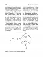
One observation: it is another indication for the 'smartness' of PW and the elegance of the design that he managed to completely and clearly explain a totally new concept in just 3 pages. Including figures. Chapeau.
Jan
Yay! 🙂It seems to me that we are making progress.
Yes with this caveat:If I understand your post correctly, you don't deny that the distortion of the dumpers is (largely) cancelled, you just wonder whether there isn't a more straightforward way to get rid of their distortion.
I define cancellation to be when one non-linear component is combined with another non-linear one with some complementary characteristics, additively. Like adding or subtracting numbers in a spreadsheet or using Reed-Solomon to correct digital bit errors.
I define negative feedback to always reduce distortion ratiometrically. Distortion can never be removed but only altered and, of course, re-synthesized into spectra that would not otherwise be present. There is no cancellation by my definition: cancellation is impossible! There are some folks with temporary brain failure who invoke the "Infinity God" and fool themselves, and others, into thinking their NFB scheme cancels something. No.
My position is that the Quad circuit does not cancel anything. It entirely uses NFB to reduce the non-linearities caused by the dead band between the power transistors.
So yes, my question is if we started from scratch to deal with the dead-band using NFB would we choose Quad's topology?
Yes.There certainly is in my oversimplified model, but that's due to it being oversimplified. I implicitly assumed the class-A part to have nullor properties: infinite voltage, current, transadmittance and transimpedance gain and no clipping limits. If it really had those properties, you wouldn't need the dumpers at all, you could just put a feedback loop around the class-A part and be done with it.
Yes.Slightly less theoretical but still quite unrealistic, when the class-A part has a finite transconductance but infinite output impedance and the dumpers have no collector-base capacitance (assuming they are simple emitter followers), you could just connect the class-A part to the dumpers, put a feedback loop around the combination and that's it. I think this is what you are suggesting to do.
Yes. It is a transconductance amplifier so dc voltage gain will not be an issue. As the f increases the error voltage at the input will increase in size due to limited bandwidth of the transconductance amp.The problem is that in reality the class-A part will have a large but finite voltage gain, so you get a dead zone, a range of input voltages where the feedback loopgain (practically) drops to zero and the amplifier (practically) doesn't react to the input at all. For example, when the voltage gain is 100 000 and the dumper transistors need 700 mV to start conducting, input voltages up to 7 uV will not result in any output. In real life the gain of the class-A part drops with frequency, so this issue will get more severe with increasing frequency.
Yes.You can mitigate this to some extent with a resistor bypassing the base-emitter junction of the dumpers, making an extra path from the class-A amplifier straight to the output. At least the loopgain then drops to a non-zero value when the signal is too small to make the dumpers conduct. This works, but you still have a very nonlinear thing inside your feedback loop and only have the loopgain to correct for its distortion. Especially at high frequencies, where loopgain drops, it will be difficult to get a reasonably low distortion out of it.
Yes.The nice thing about Quad's current dumping is that the gain of the class-A part is allowed and even supposed to drop with frequency. Otherwise it can't balance out the path through the inductor, which also drops with frequency.
At low frequencies, where the inductor is essentially a short circuit and the 120 pF capacitor an open branch, your Fig. Q1 is simply a feedback amplifier with class-C output stage having a 47 ohm bypass resistor between base and emitter of the transistors of the class-C stage.
No. 😀At higher frequencies, the gain of the class-A part drops. In a normal feedback amplifier with class-C output stage having a 47 ohm bypass resistor between base and emitter of the transistors of the class-C stage, the gain drop would 1:1 result in a distortion increase. In Quad's version the distortion increase is much reduced, because the trick with the extra inductor ensures that the class-C stage's distortion is still cancelled out.
Again, there is no cancellation going on.
The balanced bridge only means that BJT Vbe variations do not add to the feedback signal but they are still there and appear at the class-A amplifier's output just like they would with no bridge. The BJT hfes also change the system loop gain just like they would in a conventional topology.
Please do explain again if I am missing something. 🙂
At the moment, I don't see a theoretical advantage to the Quad circuit but see these disadvantages:
The possibility of Vbe distortion corrupting the feedback if the bridge is not perfectly balanced.
A big inductor in the emitters - this impedes fast current delivery and creates EMI.
Jan, before you stroke out with admiration and fall and hurt yourself, I think I should highlight a couple of claims that Peter Walker makes in that article.That works Ian, thanks!
One observation: it is another indication for the 'smartness' of PW and the elegance of the design that he managed to completely and clearly explain a totally new concept in just 3 pages. Including figures. Chapeau.
Jan
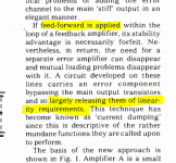
1) He places a 47 ohm resistor in parallel with the base-emitter of some transistors and calls this "feed-forward".
2) He claims that this 47 ohm resistor, in between his amp and the speaker, is able to largely relieve the power transistors of any need to be linear.
Smartness alright; he sold a lot of Quad 405s. 😉
Attachments
Jan, before you stroke out with admiration and fall and hurt yourself, I think I should highlight a couple of claims that Peter Walker makes in that article.
1) He places a 47 ohm resistor in parallel with the base-emitter of some transistors and calls this "feed-forward".
2) He claims that this 47 ohm resistor, in between his amp and the speaker, is able to largely relieve the power transistors of any need to be linear.
Smartness alright; he sold a lot of Quad 405s. 😉
So now you resort to misquoting Peter Walker? He doesn't state anywhere that current dumping is just placing a resistor between base and emitter, because it isn't.

I define cancellation to be when one non-linear component is combined with another non-linear one with some complementary characteristics, additively. Like adding or subtracting numbers in a spreadsheet or using Reed-Solomon to correct digital bit errors.
I don't. When two paths have the same transfer except for opposite signs and sum up to zero, that's also cancellation as far as I'm concerned. In this case the distortion of one part of the circuit ends up on the output through two paths that (largely) cancel each other in this sense.
Please do explain again if I am missing something. 🙂
If you still don't get it, I'm afraid it's hopeless.
At the moment, I don't see a theoretical advantage to the Quad circuit but see these disadvantages:
The possibility of Vbe distortion corrupting the feedback if the bridge is not perfectly balanced.
A big inductor in the emitters - this impedes fast current delivery and creates EMI.
Even in very conventional amplifiers, inductors are often used at amplifier outputs to make them less sensitive to load variations and to suppress interference picked up by the loudspeaker cables.
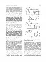
Baxandall's analysis (from Talbot-Smith's book) :


Attachments
Last edited:
Ok I know I'm rustling feathers by poking this sacred cow. I am sorry. But what would you have me do?
I see errors or oversights in all these papers. I see gross exaggerations in PW's description that I would not expect to be tolerated except perhaps in commercial audio where everything seems to be allowed especially if it looks unusual and stirs interest.
Do you want to understand the reality behind stuff or is DiyAudio a place where being awestruck is a protected characteristic?
🙂
The only gross exaggerations I've seen in this thread were those in your posts. The same holds for incorrect analyses and incorrect quotes. (My earliest posts about the Quad listening test were also wrong, of course, but I've corrected that.)
Regarding Walker's claim that the dumpers in a current dumping topology need not be linear: he backs that up with an amplifier achieving <0.01 % distortion with a class-C dumper stage.
Regarding Walker's claim that the dumpers in a current dumping topology need not be linear: he backs that up with an amplifier achieving <0.01 % distortion with a class-C dumper stage.
Last edited:
I rather know the answer
but
is there a simply way to rework standard amplifier to implement in it bridge nfb circuitry
to obtain similar to Q405 amp?
but
is there a simply way to rework standard amplifier to implement in it bridge nfb circuitry
to obtain similar to Q405 amp?
This post contains spoilers
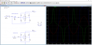
I've knocked up a couple of LTSpice circuits for anyone to play with so you can see for yourselves what is really going on.
The top circuit is a simplified version of the Quad 405 based on PW's paper. It is not exactly the same as the real circuit but is good enough to show the principle of operation.
The bottom circuit is a version operating in open loop.
Note:
The yellow curve is the voltage output of the open-loop model (bottom). It is not linear at all as you should expect. The Quad does not add any non-linear components that could cancel this distortion away so instead relies on a lot of NFB to reduce it. The Quad's transconductance amplifier (aka class A amplifier) has to output a very distorted current to compensate and this is generated entirely by NFB.
The blue curve is the transconductance amplifier's current output in the closed-loop model (top). You can see it is extremely distorted. The power transistor distortion has not been cancelled. The high NFB reduces the distortion at the output (red curve).
Attachments
Last edited:
Pawel,I rather know the answer
but is there a simply way to rework standard amplifier to implement in it bridge nfb circuitry to obtain similar to Q405 amp?
There was one 2013 by Apexaudio here
Current Dumping Amplifier
I've knocked up a couple of LTSpice circuits for anyone to play with so you can see for yourselves what is really going on.
The top circuit is a simplified version of the Quad 405 based on PW's paper. It is not exactly the same as the real circuit but is good enough to show the principle of operation.
The bottom circuit is a version operating in open loop.
Note:
The yellow curve is the voltage output of the open-loop model (bottom). It is not linear at all as you should expect. The Quad does not add any non-linear components that could cancel this distortion away so instead relies on a lot of NFB to reduce it. The Quad's transconductance amplifier (aka class A amplifier) has to output a very distorted current to compensate and this is generated entirely by NFB.
The blue curve is the transconductance amplifier's current output in the closed-loop model (top). You can see it is extremely distorted. The power transistor distortion has not been cancelled. The high NFB reduces the distortion at the output (red curve).
For f -> 0 it indeed becomes a simple negative-feedback amplifier, as I already mentioned at the end of post 86. What's more interesting is what happens at higher frequencies and how the distortion at the output then compares to the case without the inductor.
Last edited:
- Home
- Amplifiers
- Solid State
- Peter Walker and his current dumping principle