The point of not using the WaveIO is to find out where the problem is (PS or WaveIO)
the 12 Volt is not critical, but also best to adjust under load and after 30 minutes warm up to adjust again.
The waveIO will not work with 4 volts. seems there is something wrong with the PS at fierst glance. so it is good to measure the Dc voltage at the fuse to start with (under load)
the 12 Volt is not critical, but also best to adjust under load and after 30 minutes warm up to adjust again.
The waveIO will not work with 4 volts. seems there is something wrong with the PS at fierst glance. so it is good to measure the Dc voltage at the fuse to start with (under load)
DDDAC Noisy
hi,
i bought a 2 board dddac and it ready assembled. it sounds already pretty good... but...
i have a very high noise floor. it is mor white nois... so more high frequencies than low frequencies. any idea?
th noise is i would say maybe double to what i had with my very old morgan dac, so i hope this is not normal.
after assambling the main board i have 2 10kO resistors left... but no more free space to solder them.
i feed the dddac with spdif. 44.1 to 192khz with 24 bits
any help is appriciated!
greetings
christian
I already answered the mail you sent me. You are connecting the DAC straight to the end amplifier and using digital volume control. This causing it as the no digital filter concept gives higher quantization noise at low FS in the audio band. I suggested a -20db switch at the entry of the amplifier or at the DAC output. I also expect that the total gain is too high in your system. Are you actually able to play music round 0dbFS ? Or do you blow your speakers away ? What level are you playing normally? I mean volume -xdB at the volume control in your player ?
The point of not using the WaveIO is to find out where the problem is (PS or WaveIO)
the 12 Volt is not critical, but also best to adjust under load and after 30 minutes warm up to adjust again.
The waveIO will not work with 4 volts. seems there is something wrong with the PS at fierst glance. so it is good to measure the Dc voltage at the fuse to start with (under load)
Hi Doede,
I got a 13 ohm resistor and tested under load:
No load - 5v at gnd, 12.76v at fuse
Under load - 2.9v at gnd, 9.84v at fuse
Hi Doede,
sorry for double "posting" but i didn't knew, that you are also direct support of the DDDAC 😉
So what i did now is: Upsampling... and noise is gone 😉
Depending on the Track, i can here at 0dB but i am sitting just ~2 meters in front of the speakers... so noise on 44.1 is quit strong... but it seems upsampling is the solution 😉
Greetings
Christian
Hi Doede,
i solved another problem in my chain. Until this morning i used the SPDIF input and had a very strong noise in the speakers during changing the sample frequencys. Today i changed to i2s input... and its fine 😉

Greetings
Christian
i solved another problem in my chain. Until this morning i used the SPDIF input and had a very strong noise in the speakers during changing the sample frequencys. Today i changed to i2s input... and its fine 😉
Greetings
Christian
Hi Doede,
I got a 13 ohm resistor and tested under load:
No load - 5v at gnd, 12.76v at fuse
Under load - 2.9v at gnd, 9.84v at fuse
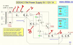
ok, there is something going very wrong after the mod here,
can you now measure on the following points with and without load and post back? (so I expect 16 values)
please measure all values against the GND output terminal
Attachments
ok, there is something going very wrong after the mod here,
can you now measure on the following points with and without load and post back? (so I expect 16 values)
please measure all values against the GND output terminal
Here are my measurements, looks like the issue is around the point 7 area.
Load NoLoad
1 9.80 12.58
2 9.74 12.58
3 9.74 12.58
4 9.72 12.60
5 3.84 5.04
6 3.81 5.04
7 6.84 12.58
8 5.11 9.55
Here are my measurements, looks like the issue is around the point 7 area.
Load NoLoad
1 9.80 12.58
2 9.74 12.58
3 9.74 12.58
4 9.72 12.60
5 3.84 5.04
6 3.81 5.04
7 6.84 12.58
8 5.11 9.55
Same issue with the 12V as well:
Load NoLoad
1 17.35 20.90
2 17.35 20.90
3 17.35 20.90
4 17.35 20.90
5 9.83 11.96
6 9.85 11.96
7 13.03 20.90
8 11.15 17.29
Here are my measurements, looks like the issue is around the point 7 area.
Load NoLoad
1 9.80 12.58
2 9.74 12.58
3 9.74 12.58
4 9.72 12.60
5 3.84 5.04
6 3.81 5.04
7 6.84 12.58
8 5.11 9.55
ok, let's start with this one...
still not logical...
The voltage drop suggest a very high current between point 1 and 2 there is 0.06 Volt drop with 0,1 Ohm -> 0,6 A.
Between 2 and 3 there is no voltage drop any more, so NO current.
Which does not make sense. The 0,6A must go somewhere. in C1? Pls check C1 / soldering
Point 8 should be GND, you should NOT measure anything more than (close to ) zero...
wrong measurement? or a problem with GND track?
Pls Switch OFF and measure OHM between point all points and GND terminal pls?
Last edited:
ok, let's start with this one...
still not logical...
The voltage drop suggest a very high current between point 1 and 2 there is 0.06 Volt drop with 0,1 Ohm -> 0,6 A.
Between 2 and 3 there is no voltage drop any more, so NO current.
Which does not make sense. The 0,6A must go somewhere. in C1? Pls check C1 / soldering
Point 8 should be GND, you should NOT measure anything more than (close to ) zero...
wrong measurement? or a problem with GND track?
Pls Switch OFF and measure OHM between point all points and GND terminal pls?
Hi Doede, I may have measured incorrectly, but regardless your mention of C1 caused me to look at the PCB traces and I realized that not all points on the positive side of C1 & C2 are connected. When I rotated the caps to the rear most positive hole and tested, it worked! Both PSU boards are calibrated and providing the correct voltage under load. Also added some Black Gates to the Mainboard and it sounds incredible.
Thank you so much for your help and for creating these board kits for the DIY community, its been a fun learning experience. I'll be sure to post pictures when completed and in its final enclosure.
Take care,
Per
Hi per,
I am glad I could help and the way it was done is very general, fact finding (measuring), deducting and based on that insight check the work.
Happy listening !
Diminishing returns?
I'm just wondering how much of a step up in SQ you get by going from 2 boards to 4 boards? Anyone with experience of making that change?
...I agree too and even better the more DAC boards you have. The extra gain the Sowters give also help a lot.
I'm just wondering how much of a step up in SQ you get by going from 2 boards to 4 boards? Anyone with experience of making that change?
On the Creative Audio website you can download a construction manual for the main board, but it's in Dutch. Is there an English version somewhere?
How about dddac.com?On the Creative Audio website you can download a construction manual for the main board, but it's in Dutch. Is there an English version somewhere?
Gesendet von meinem D5803 mit Tapatalk
How about dddac.com?
Gesendet von meinem D5803 mit Tapatalk
😎
http://www.dddac.com/documents/dddac1794_pbt_construction_manual_en_v2.pdf
http://www.dddac.com/documents/dddac1794_pbt_construction_manual_en_v2.pdf
Hi,
Little confusion here. The above referenced document states trimming the dac module to 40mV between the test point and the analogue common on the main board.
This document http://www.dddac.com/documents/dddac1794pbt_nos_ver51.pdf however states NOT to use the common on the main board (but use the common on the dac module I presume)
What is the correct procedure for trimming?
Steef
Hi,
Little confusion here. The above referenced document states trimming the dac module to 40mV between the test point and the analogue common on the main board.
This document http://www.dddac.com/documents/dddac1794pbt_nos_ver51.pdf however states NOT to use the common on the main board (but use the common on the dac module I presume)
What is the correct procedure for trimming?
Steef
both are correct, but the common on the DAC board itself will be the most precise when you have more than one DAC board.
- Home
- Source & Line
- Digital Line Level
- A NOS 192/24 DAC with the PCM1794 (and WaveIO USB input)