IanHegglun, could I beg you to post pics of each circuit and the mod as you describe them.
I've downloaded several of your ZIP files but are thoroughly confused as to which is which.
Which circuit is your original cross-conduction query about?
Which one has good performance out to 200kHz with minimal bias?
Which one(s?) have problems switch off?
I'm sure Jan won't mind your posting a pic or 2 from your own papers in LA
Article availability?
When would you expect Ian's latest article from Volume 13 to be available for purchase and download? Some of us don't mind paying authors/publishers for original useful articles. Don't want to buy paper as I have accumulated 40 years worth of photocopied technical literature.
Regards ...
No I don't.
Jan
When would you expect Ian's latest article from Volume 13 to be available for purchase and download? Some of us don't mind paying authors/publishers for original useful articles. Don't want to buy paper as I have accumulated 40 years worth of photocopied technical literature.
Regards ...
IanHegglun, could I beg you to post pics of each circuit and the mod as you describe them.
I've downloaded several of your ZIP files but are thoroughly confused as to which is which.
Which circuit is your original cross-conduction query about?
Hi kgrlee,
This thread was intended to be for the Linear Audio CSD amp. Sorry, this this thread has lost the plot a bit. I'm new to diyAudio and obviously have a lot to learn about these threads.
My Linear Audio CSD amp fix has actually not been discussed yet. I posted a circuit I bench tested in post #89 p9.
Most of the posts have been on Wim de Jager's amp and Faran & Fulks amp; which is OK by me because they are both Current Source Driven (CSD).
Which one has good performance out to 200kHz with minimal bias?
The Faran amp was simulated out to 200kHz and it did not have a cross-conduction problem in the original circuit. This is because the two bases of the power transistors are directly connected together (that's right, no bias generator or resistor between the bases for this output stage - very unconventional).
I posted the Faran amp zero-cross region at 50Hz in post #98 waveforms.
Notice the zero-cross region is not discontinuous as you might expect with this low frequency. To me it looks like the continuity is due in part to the negative current from the charge being pulled out.
The emitter follower OPS appears to be a better choice than a common emitter OPS when they are current driven. That's because crossover in common collector is not discontinuous when current driven and when the bases are shorted together. I haven't seen anyone who has shown this result before -- so it is probably news to most.
Having said that, I'm not planning on abandoning the search for a simple way to remove the base charge in my Linear Audio amp which uses common emitter power transistors. The Linear Audio amp's common emitter power transistors allows easy paralleling (no emitter resistors are needed for current sharing) to get to very high powers, while the Faran amp doesn't allow easy paralleling of power transistors and is limited to around 50W/8R (unless some clever idea can overcome this).
Which one(s?) have problems switch off?
The Linear Audio CSD amp and Win de Jager amps have switch-off problems, seen as a high idle current with no load when driven at full swing and a high frequency. Both the Linear Audio CSD amp and Win de Jager amps are limited to about 40kHz under the above test conditions.
As mentioned in my article this is not a problem for use in most audio applications since tweeters are not rated for full continuous power, so it is only a problem during bench testing, or if something goes wrong with the input shielding and your amp oscillates above 20kHz without the load connected and you don't notice it until it over heats. That's why I recommend a thermal cut-out switch for my CSD amp on the heatsink to turn off the mains if it overheats.
Still, I am hoping to find a simple addition to my published Linear Audio CSD amp that keeps the no load idle current down to acceptable levels at full output with no load even to 100kHz.
BTW I have just done bench tests on an improved charge pull-out circuit on my Linear Audio CSD that is simple and keeps the no load idle current down to acceptable levels. I hope to post a circuit update soon.
The published Linear Audio CSD amp circuit is already on the Linear Audio site in the Oops section (since I inadvertantly reversed the PNP and NPN power transistors -- my bad, sorry all, not the Editor's fault).
When would you expect Ian's latest article from Volume 13 to be available for purchase and download? Some of us don't mind paying authors/publishers for original useful articles. Don't want to buy paper as I have accumulated 40 years worth of photocopied technical literature.
Regards ...
Should be available now:
https://linearaudio.net/volumes/2282
Jan
Still have access probelm
Thanks. Placed order, but only able to access article_placeholder.pdf.
Thanks. Placed order, but only able to access article_placeholder.pdf.
An improved charge pull-out circuit for the Linear Audio CSD amp
Attached is the promised improved charge pull-out circuit mods for the Linear Audio CSD amp that I bench tested. Only one of the two output pair are shown for clarity.
The added components are in the 3 dotted areas. Cc is a coupling capacitor that sends a reverse voltage to the opposite side when one side turns on - let's say QM16 is turning on then QM13 gets a lift in the voltage to Q1's base, thereby causing Q1 to discharge QM13's base charge. C5 across D5 slows Q1 for stability.
BTW Cc can be fairly small, only 1nF to 10nF, because Cc feeds the high resistance R7 (notice D5 is reverse biased when Q1 conducts).
A simulation plot at 50kHz into 8 ohms is attached. Ib(Qm13) shows 17mA peak negative base current flows via Q1 over about 2us. The rail current I(V2) shows there is not much cross-conduction (where the current plots cross).
For my bench tests I used the values shown and the idle current increased from 80mA to 120mA with no load and full swing square wave up to 130kHz (the limit of my oscillator). This is what I have been looking for. Simple and effective and no extra rail voltages.
I hope to do some THD tests. When I am happy all's well with this idea I'll post the full simulation circuit.
Hi All,...I have just done bench tests on an improved charge pull-out circuit on my Linear Audio CSD that is simple and keeps the no load idle current down to acceptable levels. I hope to post a circuit update soon.
Attached is the promised improved charge pull-out circuit mods for the Linear Audio CSD amp that I bench tested. Only one of the two output pair are shown for clarity.
The added components are in the 3 dotted areas. Cc is a coupling capacitor that sends a reverse voltage to the opposite side when one side turns on - let's say QM16 is turning on then QM13 gets a lift in the voltage to Q1's base, thereby causing Q1 to discharge QM13's base charge. C5 across D5 slows Q1 for stability.
BTW Cc can be fairly small, only 1nF to 10nF, because Cc feeds the high resistance R7 (notice D5 is reverse biased when Q1 conducts).
A simulation plot at 50kHz into 8 ohms is attached. Ib(Qm13) shows 17mA peak negative base current flows via Q1 over about 2us. The rail current I(V2) shows there is not much cross-conduction (where the current plots cross).
For my bench tests I used the values shown and the idle current increased from 80mA to 120mA with no load and full swing square wave up to 130kHz (the limit of my oscillator). This is what I have been looking for. Simple and effective and no extra rail voltages.
I hope to do some THD tests. When I am happy all's well with this idea I'll post the full simulation circuit.
Attachments

A question
Are those open loop results with no negative feedback? Looks very promising.
Hi All,
A simulation plot at 50kHz into 8 ohms is attached. Ib(Qm13) shows 17mA peak negative base current flows via Q1 over about 2us. The rail current I(V2) shows there is not much cross-conduction (where the current plots cross).
Are those open loop results with no negative feedback? Looks very promising.
Are those open loop results with no negative feedback? Looks very promising.
That's closed loop. About 16dB of nfb at 50kHz. See AC plots for OL and CL attached.
Attachments
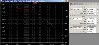
I am reading your graph of gains correctly?
So what is the closed loop gain at 180 degrees phase? My reading of the graph is that it is greater than 0 dB.
Thanks for these results.That's closed loop. About 16dB of nfb at 50kHz. See AC plots for OL and CL attached.
So what is the closed loop gain at 180 degrees phase? My reading of the graph is that it is greater than 0 dB.
...So what is the closed loop gain at 180 degrees phase? My reading of the graph is that it is greater than 0 dB.
Yes, well spotted. I noticed that before I sent it. Not sure why it still runs in .trans without oscillating even though the phase margin says it should oscillate!?
A mystery. Other members may have some answers.
Whatever it is, it's a reminder that SPICE has surprises now and then.
One possibility is the input stage MOSFET models drain conductance and capacitance model gives different GBW in .op (for AC operating point) and .trans (large signal operation).
BTW The values for the compensation components in the simulation are close (+/-20%) to the values for my bench test but the models are not matched to the actual semiconductors of my bench version (maybe +/-30%). But still, this cannot explain why my negative phase margin in AC analysis doesn't oscillate in my .trans simulations.
I haven't looked at the plot, but in general, feedback systems can be stable with a phase shift greater than 180 degrees at a frequency where the loop gain is greater than unity, just as long as the phase returns to a safe value before the loop gain becomes 1. They call that conditional stability. See the Nyquist stability criterion.
...A mystery. Other members may have some answers....
I haven't looked at the plot... They call that conditional stability. See the Nyquist stability criterion.
The phase in Ian's plots looks to fall montonically so conditional stability is not the explanation in this case.
Ian, I don't understand exactly what you have plotted but it looks like you have not correctly included internal loops.
This is a common difficulty, if you use a Tian probe then you can show us exactly where the loop gain is calculated.
Best wishes
David
Oops ... A slight error.
Sorry all. I meant to look at the open loop gain instead of the closed loop gain.
Yes, well spotted. I noticed that before I sent it. Not sure why it still runs in .trans without oscillating even though the phase margin says it should oscillate!?
Sorry all. I meant to look at the open loop gain instead of the closed loop gain.
Have a look at the response to a square wave input
It might be interesting to see the output waveform with a 20 kHz square wave input.
A mystery. Other members may have some answers.
It might be interesting to see the output waveform with a 20 kHz square wave input.
It might be interesting to see the output waveform with a 20 kHz square wave input.
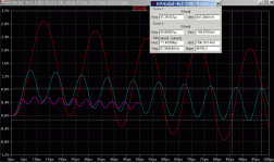
The 20kHz squarewave response is attached (first one). Same circuit as the previous gain/phase plots.
The second plot is with no phase advance capacitor (C13) 56pF across the feedback resistor. I thought that may be stopping oscillation by providing some phase advance but without it we get ringing but not steady state oscillation.
The third plot is where the input frequency is stepped 50kHz, 100kHz and 200kHz in open loop with 5mV peak input. From this the gain at each frequency can be calculated and compared to the previous AC gain/phase values.
I calculated 40.2dB at 100kHz and 26.6dB at 200kHz for the .trans run. The AC gain/phase plots show 40.0dB and 26.1dB respectively which are very close.
Also the .trans phases at 100kHz and 200kHz were 172 deg at 100kHz and 205 deg at 200kHz. The AC gain/phase plots show 174.6 deg and 205 deg respectively which are also very close. These were measured by plotting d(V(out)) to find the zero cross (now at the peaks) for the 9th cycle.
So it appears the .trans simulations correspond to what the .AC simulations show on the gain/phase plots. Which means there must be some other reason why it doesn't oscillate. And it doesn't appear to be the phase advance capacitor because without it there's still no oscillation.
It's still a mystery; more a curiosity, why is it so?
I'll place a zip file 'BiModal-4v1-CSD-fix2a-sims_03-May-2017.zip' on myDrive (link in signature) in the diyAudio directory. You can generate the same plots as my ones here. These circuits have the improved charge pull-out mods.
Attachments


Thanks. Placed order, but only able to access article_placeholder.pdf.
Fixed.
A question?
I don't have the complete circuit here yet but the square wave response plots are a bit unusual in that they are asymmetrical. On the second plot why is there ringing only on one voltage transition?
Perhaps there is some sort of asymmetry on the CMOS gates?
From what I remember your circuit is basically symmetrical. The square wave input is symmetrical about 0 vdc. You have tried running the simulation longer to eliminate any startup transients?
OK I have the simulation file and will do some investigations tomorrow.
It's still a mystery; more a curiosity, why is it so?
I don't have the complete circuit here yet but the square wave response plots are a bit unusual in that they are asymmetrical. On the second plot why is there ringing only on one voltage transition?
Perhaps there is some sort of asymmetry on the CMOS gates?
From what I remember your circuit is basically symmetrical. The square wave input is symmetrical about 0 vdc. You have tried running the simulation longer to eliminate any startup transients?
OK I have the simulation file and will do some investigations tomorrow.
Some results
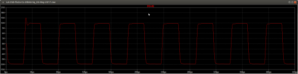
With C13 removed the ringing you plotted is transient. If you extend the simulation duration it disappears. ie
Modify the voltage source to something vaguely like:
PWL REPEAT FOREVER(0m 0 {tramp/2} {-Vpk} {tramp/2+0.5/f} {-Vpk} {3*tramp/2+0.5/f} {+Vpk} {3*tramp/2+1/f} {+Vpk} {5*tramp/2+1/f} {-Vpk}) ENDREPEAT
and extend the simulation time.
Then you will get a plot as shown in the attached file. Looks like it is going to drop below freezing tonight here in Melb.
The second plot is with no phase advance capacitor (C13) 56pF across the feedback resistor. I thought that may be stopping oscillation by providing some phase advance but without it we get ringing but not steady state oscillation.
With C13 removed the ringing you plotted is transient. If you extend the simulation duration it disappears. ie
Modify the voltage source to something vaguely like:
PWL REPEAT FOREVER(0m 0 {tramp/2} {-Vpk} {tramp/2+0.5/f} {-Vpk} {3*tramp/2+0.5/f} {+Vpk} {3*tramp/2+1/f} {+Vpk} {5*tramp/2+1/f} {-Vpk}) ENDREPEAT
and extend the simulation time.
Then you will get a plot as shown in the attached file. Looks like it is going to drop below freezing tonight here in Melb.
Attachments
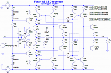
Faran mods for Class-AB
Hi All,
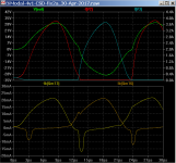
Adding a second parallel Class-B stage (bases shorted) allows source idle current in one Class-B stage and sink idle current in the second Class-B stage. This creates a composite output stage that behaves like Class-AB while retaining shorted bases in each stage. See that attached circuit.
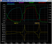
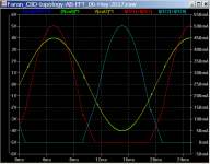
As mentioned in previous posts, shorted bases allows fast charge pull-out without cross conduction. See the attached simulation at 200kHz. The idle current is 70mA. The third plot shows the crossover region at 50Hz and 1W/8R. The weighted THD can be reduced to 0.5% (which is below the audible threshold) with an input stage with 40dB of nfb (the unweighted THD is then 0.003% at 1W).
This Faran-AB approach allows the distortion at low power to fall off below 1W with 70mA of idle current. Without this modification the Faran-B approach gives increasing distortion below 1W which is unacceptable for Hi-Fi amps. So now Faran-AB approach can be used for Hi-Fi.
And I should mention the output stage linearity is not affected by temperature changes in the power transistors, and there's no need for a bias current trimpot.
The circuit as shown is not buildable as is since different HV driver transistors are required for a 100W amp. But it wouldn't take much more work to finalise it and build one. It probably needs a new thread. Anyone interested in taking it up? I have enough to do already.
I will place the simulation file on myDrive (link in sig line) in the diyAudio folder that generated the plots shown here.
Cheers,
Ian Hegglun
...There may be some mods that could get the wTHD lower. Any suggestions? Also mods for standard dual-rail operation.
Hi All,
Adding a second parallel Class-B stage (bases shorted) allows source idle current in one Class-B stage and sink idle current in the second Class-B stage. This creates a composite output stage that behaves like Class-AB while retaining shorted bases in each stage. See that attached circuit.
As mentioned in previous posts, shorted bases allows fast charge pull-out without cross conduction. See the attached simulation at 200kHz. The idle current is 70mA. The third plot shows the crossover region at 50Hz and 1W/8R. The weighted THD can be reduced to 0.5% (which is below the audible threshold) with an input stage with 40dB of nfb (the unweighted THD is then 0.003% at 1W).
This Faran-AB approach allows the distortion at low power to fall off below 1W with 70mA of idle current. Without this modification the Faran-B approach gives increasing distortion below 1W which is unacceptable for Hi-Fi amps. So now Faran-AB approach can be used for Hi-Fi.
And I should mention the output stage linearity is not affected by temperature changes in the power transistors, and there's no need for a bias current trimpot.
The circuit as shown is not buildable as is since different HV driver transistors are required for a 100W amp. But it wouldn't take much more work to finalise it and build one. It probably needs a new thread. Anyone interested in taking it up? I have enough to do already.
I will place the simulation file on myDrive (link in sig line) in the diyAudio folder that generated the plots shown here.
Cheers,
Ian Hegglun
Attachments
Last edited:
- Status
- Not open for further replies.
- Home
- Amplifiers
- Solid State
- Current-Source-Driven-power-transistors-and-mitigating-cross-conduction-distortion