Boys, Hello.
It has long been looking for a theme. Acquired miniDSP, but I did not like the built-in DACs - sold. Found freeDSP project. But I want to use only the digital part, the analog to disconnect.
I ask you to criticize my idea, because I want to make the printed circuit board itself.
Source: optical converter with output I2S 48kHz
Then it is transferred to the ADAU1701.
From adau published 6 digital channels on external DACs.
Masterklok will be distributed from the generator.
It will be supplied to the DAC 6 and adau1701.
Adau will work as a crossover.
Question. Does this scheme the right to life?
And to clarify: LRСK signals and BCK from the source drive to the adau, and then DACs to take them from adau?
Or these signals from the source to guide and Adau and DACs?
Thanks
I think the biggest hurdle I've run up against is the clocking. Specifically, I want to get I2S audio input. To do that, I understand, that the ADAU1701 needs to be driven from the same clock source as the I2S source.
The classic boards provides a mclk in and the ability to toggle is via a jumper, so cool so far. The problem is that this needs to be exactly 256 x lrclock, as the board doesn't have jumpers for setting PLL_MODE0 and PLL_MODE1 (they're hard wired to 0 and 1). My I2S source is using a 512xrlclock mclk. I can't really change my I2S source (and frankly, it's got the better clock anyways). Any ideas on how I could rectify this without having to hack vcc onto PLL mode0?
The classic boards provides a mclk in and the ability to toggle is via a jumper, so cool so far. The problem is that this needs to be exactly 256 x lrclock, as the board doesn't have jumpers for setting PLL_MODE0 and PLL_MODE1 (they're hard wired to 0 and 1). My I2S source is using a 512xrlclock mclk. I can't really change my I2S source (and frankly, it's got the better clock anyways). Any ideas on how I could rectify this without having to hack vcc onto PLL mode0?
gustavus,
where is the I2S clock coming from? if it's coming from a serial stream, that clock is always worse than the crystal clock from the ADAU. you will needs sample rate converters even for identical but out of phase signals. the adau DAC's are sensitive to clock degradation, and that's why the adau or any other DAC likes to be clocked by a crystal quality clock. if your I2S mclk clock is rock solid you can divide it by 2 and feed it into the mclck of the freedsp board. the PLL settings are set to generate the 50M internal clock. I once made the error of setting the pll mode jumpers wrong and found the chip was running at 100mips, but this overclocking it is not a guaranteed operation. I checked that with analog devices adn they confirmed it.
where is the I2S clock coming from? if it's coming from a serial stream, that clock is always worse than the crystal clock from the ADAU. you will needs sample rate converters even for identical but out of phase signals. the adau DAC's are sensitive to clock degradation, and that's why the adau or any other DAC likes to be clocked by a crystal quality clock. if your I2S mclk clock is rock solid you can divide it by 2 and feed it into the mclck of the freedsp board. the PLL settings are set to generate the 50M internal clock. I once made the error of setting the pll mode jumpers wrong and found the chip was running at 100mips, but this overclocking it is not a guaranteed operation. I checked that with analog devices adn they confirmed it.
gustavus,
where is the I2S clock coming from?
I'm actually stealing the signal from my Schiit Modi 2 (USB DAC). It has a CM6631A being which I believe is being fed by XOs Y1 and Y2 (there's another XO X1 which is a 12mhz part for USB clocking as well). Long story, but basically my project is a USB --I2S--> DSP --I2S--> DAC. I tested the onboard ADC/DAC on the FreeDSP board and everything was just fine - so I moved onto testing I2S and needed a source. Instead of going out and buying a premade board I went to see if I had any I2S sources and realized the MODI 2 contained provisions for me to solder headers onto for capturing I2S. I haven't traced the PCB to see if the master is directly from the XO or if its derived from it and provided by the CM6631A (I don't think I saw anything in the datasheet about it being capable of this, however). Here's the I2S source, master clock signal, and lrclock signals:
Edit: I looked at the data sheet and it looks like y1/y2 are 49mhz clocks feeding xd6/xd7 on the cm6631a so the 24mhz mclock signal is generated from from the cm6631a which I'm sure is referenced from xd6/xd7?
Attachments
Last edited:
well you could clock the freedsp with the 22.5792Mhz mclk from the modi2 , but that clock needs to be always there. you cannot change the source from 44.1 to 48khz on the fly as the pll will need to re-stabilize.
you also need to set the PLL jumpers (currently hardwired) to 2x to get the 45mips.
you also need to set the PLL jumpers (currently hardwired) to 2x to get the 45mips.
well you could clock the freedsp with the 22.5792Mhz mclk from the modi2 , but that clock needs to be always there. you cannot change the source from 44.1 to 48khz on the fly as the pll will need to re-stabilize.
you also need to set the PLL jumpers (currently hardwired) to 2x to get the 45mips.
Yeah that's the challenge. I'm going to figure out how to lift PLL_MODE0 and short it to PLL_MODE1 to set mclk to be 512*fs.
you can lift pin 37 and 38 at the same time by sliding a sharp tweezer in from the side, then bend pin 37 back and reconnect.
pin 38 can be carefully bent over to 39.
I gave that a good try - but no luck. I just ended up destroying one of my boards.
") I clearly don't have the right hand for that detailed of work.
I clearly don't have the right hand for that detailed of work.That said - I DID get it to clock from an external clock: when doing 192khz out on the modi2, BCLK is 12.288MHz. Score, I can just split that between BCLK and MCLK - and everything will be in sync.
Only one problem, I discovered that BCLK is outputting 3.3V (in fact all of the serial in ports are outputting 3.3V). I traced them back to the chip, and the PCB is correct so now I'm just confused.
Other than control registers and the schematic is there anything else I need to do to get I2S input working?
Attachments
skip coffee next time , take a half glass of wine instead to reduce the muscle tone (tip from a microsurgeon). you need a stereomicroscope, very fine pencil tip soldering iron like a weller WRMP. you'll be fine..
Woh there. You're talking to a guy who roasts his own beans in a popcorn makers to have the most hand jittery day possible.
I've given up on fixing these boards. I'm going to build some SMD boards - and put jumpers on them to set the PLL modes. Until then, I just need to get I2S audio into these two existing boards.
I just don't get what I'm missing. It's like the I2S input pins are all being configured as GPIO out pins, being held high (they all show +3.3V on them). There just doesn't appear to be any reason why
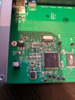
I've begun populating two FreeDSP classic boards.
I've been thinking about the, extra, A/D conversion.
I have a few IC's att home that I could use for SPDIF to I²S if any of them puts out something the ADAU1701 accept?
They are:
DIR9001, WM8804, WM8805, plus a few Cirrus chips that I don't remember now.
The Wolfson chips can be set for 16/24bit I²S out as well as 16bit right justified (I love TDA1541A).
Right now I need the FreeDSP boards to:
Pass >225Hz through to one amp and then the top of my dipole speakers.
Do dipole compensation and send 25-225hz to the second amp and then to the dipole woofers.
Today I run two pair of cables from the preamp, one pair to a DXC2496 that handles the signal to the woofers before sending it on to the amp.
It would be good if I could use REW (thinking about getting a mic) and do some room EQ:ing as well.
On another note, are there any good, in depth tutorials for Sigmastudio?
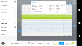
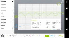
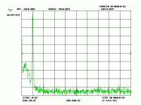
I tried syncing the adau1701 from an spdif generated Mclk. this clock is always worse than the xtal clock from the ADAU. so you will find the sideskirts of the spdif clock (pll noise bandwidth) back in the DAC output noisefloor on the LF side. better to use an SPDIF than can operate as I2S slave to the ADAU1701 as I2S master. the pic shows a pure 1khz sine generated by sigmadsp generator fed to the dac, and the LF noisefloor below 1Khz due to the rattling MCLK clock from the I2S receiver . I added an ASR to fix the problem and set the ADAU as master.
Attachments
Last edited:
The board I designed for WM8805, just got them last week, is designed so I can Jumper it as master or slave.
I also have the options for output (16/24bit I²S and 16bit right justified).
That would be a possible option as SPDIF input then?
Would it be a possible/wortwhile upgrade to use a separate XO for the adau1701? Something like the Flea or a buffered TCXO?
I also have the options for output (16/24bit I²S and 16bit right justified).
That would be a possible option as SPDIF input then?
Would it be a possible/wortwhile upgrade to use a separate XO for the adau1701? Something like the Flea or a buffered TCXO?
Guys, read again the different projects on this chip, eventually came to the embodiment described by Gustavus
 So I decided to sync problem by installing ASRC.
Question - in which Sigma studio output mode set of Adau: master or slave?
And will this scheme work?
Thanks
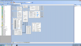
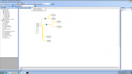
In the end, I want to try such a scheme here (sorry for the quality. I write with the phone)basically my project is a USB --I2S--> DSP --I2S--> DAC.
Question - in which Sigma studio output mode set of Adau: master or slave?
And will this scheme work?
Thanks
you only have to connect the LRCK of the DAC to the LRCK of the I2S input and the DAC BCK to the I2S in BCK . the input cannot generate the clocks, it needs it from the I2S output.
so in the ADAU register control tick the master mode in the serial output block and set the polarities and values correct. you may power down the adc's and dacs to save some current. I sometimes use the dac as a logic level output to control mute circuitry as most of the ports are already in use.
so in the ADAU register control tick the master mode in the serial output block and set the polarities and values correct. you may power down the adc's and dacs to save some current. I sometimes use the dac as a logic level output to control mute circuitry as most of the ports are already in use.
Thank you responded.
Excuse me. I forgot to clarify one point - ASRC have the output - master, in - slave.
So I think it is a source synchronous signal.
And I think that in this case, my circuit is operable. I'm right?
That is you have to offer ADAU connect output to the input, in addition?you only have to connect the LRCK of the DAC to the LRCK of the I2S input and the DAC BCK to the I2S in BCK . the input cannot generate the clocks, it needs it from the I2S output.
Excuse me. I forgot to clarify one point - ASRC have the output - master, in - slave.
So I think it is a source synchronous signal.
And I think that in this case, my circuit is operable. I'm right?
Yes. I have considered this point, so look forward to the consumption of about 60mA.you may power down the adc's and dacs to save some current.
Hmm, I do have a AD1896A IC as well (with a nice TCXO). I started on a perf board ASRC. I really don't like perf boarding more complex stuff though as I feel it looks messy.
How would one, if possible with good SQ, go about to get a digital chain up to the amps? Preamp/volume control, DSP/X-over, then do the D/A before amps and speakers?
How would one, if possible with good SQ, go about to get a digital chain up to the amps? Preamp/volume control, DSP/X-over, then do the D/A before amps and speakers?
Is there interest for SMD A version of PCB here? Anyone tested it?
Classic RCA through hole version gets a bit too busy around ADAU1701 which makes me nervous. Classic SMD A however, for some reason, is designed with 0805 components which are just too small for older people like me, so I just went at it and replaced all the 0805 with 1206_HandSoldering footprints, maintaining the same form factor. This should be sweet to work with. I am planning to order some boards soon.
Classic RCA through hole version gets a bit too busy around ADAU1701 which makes me nervous. Classic SMD A however, for some reason, is designed with 0805 components which are just too small for older people like me, so I just went at it and replaced all the 0805 with 1206_HandSoldering footprints, maintaining the same form factor. This should be sweet to work with. I am planning to order some boards soon.
Hi everyone, just come across this cool project. Has anyone compared the output quality to the minidsp? I'm using a minidsp open DRC in my active horns but I'm sure we can do better than the minidsp.
For now I'm just reading all the posts to get a feel for the project.
Interesting.....
Sent from my Moto G (4) using Tapatalk
For now I'm just reading all the posts to get a feel for the project.
Interesting.....
Sent from my Moto G (4) using Tapatalk
- Home
- Source & Line
- Digital Line Level
- freeDSP - an open source 2-in 4-out digital crossover board