I was not clear. This is not a traditional protection circuit, it's more an automatic volume limiter. Other protection must deal with faults. I assume the amp is overdriven, or the speaker wires are shorted -- user error. Those are very common events, and I wanted a clean way to deal with them.
Why bother? We do know how to make VI limiters that clamp output stages. VI limiters work -- they do prevent fires, assuming the amp works enough to clamp. But they sound awful, because with reactive loads they false trigger, chop the output and then the reactive load dumps back into the amp, typically at zero crossings. So the amp is safe, but this back emf kills tweeters and sounds trashy. Phil Anderson and Rod Elliot explained the problem here:
VI Limiters in Amplifiers
In brief, the picture below tells the story, exaggerated. Ugly, no?
My old Mission Cyrus One Amp used this concept. So I wanted to apply it here. Mission used a clamp on the LTP current source to do it, but this current feedback amp has no such control point. So, I fell back to an old idea I used in a friend's guitar amp in 1978, which I remember very well because he raved about it - it let him just play, without diddling the volume control while performing.
So here I wanted to automatically turn down the volume for a period when overcurrent was detected. I don't want the VI limiter hash, but I do want to guard against the most common fault, which is user error. This automatic volume control circuit aims to do that, with a fast attack, slow decay. Overcurrent detection is sensed by the transistor pair on the output, which make a Schmitt trigger, or thyristor, depending on how you view it. The JFET is a sort of automatic volume control, clamping the input to ground when its gate is at zero volts.
This circuit only works on a functional amp, and there must be other protection in case of failures. I assume there is a separate loudspeaker protection circuit external to the amp, and power fuses and so on, although I like your Cap multiplier much better for that. Anyway this is pretty complex, and I was hoping to keep it simple to match the simplicity of the amp. I'm not satisfied with this.
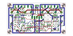
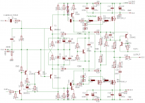
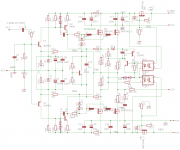
I have done a trial layout though, it's buildable on a 3x4 board, free Eagle's limit. It might fit on a 2x4 board, if I leave out stuff and use more SMD bottom side. These are paper designs, not tested, subject to change, but I'll share the current state of the schematic and board below.
Could I take the functional aspects of the protection circuit here up to the clamp JFET and connect that to the gate of my CM?
Could I take the functional aspects of the protection circuit here up to the clamp JFET and connect that to the gate of my CM?
The JFET is low power, so it's best used for clamping low level signals and not much current. I don't know what gate you mean. The MOSFET gates? Depends on the drive, most likely not. A higher power device might, not sure where to get it. I recall a National JFET that could take some current. But usually they are good for low level clamps, switches, etc.
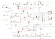
By the way I took out the op amp and made a smaller layout, 2x4. Schematic and layout below.
Attachments
All GB boards are now in the mail. Some of you might be seeing yours already today in the mail?
MOSFET gates by definition use no current for DC right? Voltage is all that matters.
Yes and no. The gate looks like a capacitor. They are amazingly well insulated. If you use a DMM to charge the gate, say, then you can take it away and measure the Drain to Source resistance. It will say on for minutes if the device is good.
So yes, voltage, but remember it's a capacitor. You have to charge it rapidly and discharge it rapidly, which does require current. Many designers use followers to drive them, which have active drive one way, resistive pulldown the other. The resistor must be small, 100 ohms or so, for fast discharge to avoid cross conduction.
But the drive voltage Vgs must go up to say 6 volts or more for full output, so the follower sources 60ma for example. Small signal Jfets won't handle that. You can use any power bipolar or mosfet though. Or control the follower base or gate, which is usually a low current node.
The design I showed has pieces that can be adapted to other drive requirements, the thyristor for instance. It's solid. I chose to drive a Jfet because it's a perfect match for the input. The stuff between is just level shifting. I had to get the floating thyristor signal from varying AC level to a ground referenced input, and I just picked one of many ways. I considered an optocoupler too.
Actually the optocoupler would be excellent for your CM. You could drive two to control both voltages. Voila, we have reinvented the solid state relay. That is one of many approaches. I used jelly bean transistors for cost savings only, but the optocoupler is more elegant.
I looked at the Capacitor Multiplier. Yes, you could incorporate turn off into it, but it might not help. Here is a schematic of the existing CM. Clamp gate to source, DC off. That would not discharge the main supply caps though, so a lot of harm could be done by that energy. The switch needs to be downstream from the main caps to prevent that. Instead of a CM, use a regulator with shutdown after the main cap. Nothing is simple...
Attachments
Sorry that "shoot through" confused you. Maybe cross conduction is the correct term. The current that passes from rail to rail when the two output devices both conduct when a signal frequency is too high to allow the devices to switch off sequentially.................
I did not understand a couple of things though. By shoot through current, do you mean cross conduction?
The monitor reads the voltage across the two source/emitter resistor in series. The voltage drop across these resistors is divided by the ratio ladder. That reduced voltage has to be high enough to trigger the Thyristor. In your sch the values are :Possibly due to input frequency too high, or Vbias not tracking, or?? Always a concern. I show fixed bias, but probably need a pot for tweaking.
And, what do you mean by "sensitivities for these are different by a factor of ~2"? I figured the original Cyrus had about a 7A trip, this was upped to about 10.5A in my implementation. Those were trial values, because I want to test this to see if it either nuisance triggers because the limit is low, or fails to trigger on harmful overcurrent.
..................
0r22 twice
150r
1k
If 7A flows from top to bottom the Vdrop (=2*Vre) is 3.08Volts. The divided voltage is 3.08*150/(150+1k0) = 401.7mV and this is what triggers the Thyristor.
There is an effect due to the RC filter built into the measurement of that 7A current. A transient current will have to charge up that capacitor. This delays triggering. The RC = 1uF*(150r||1k) ~ 0.13ms
A very fast transient would need to rise very high to trigger. A slow transient would need to rise only a little higher to trigger. A long term DC would simply need to reach the trigger threshold. Have you done a sim in LTspice to see the effect of your filter?
Now consider what happens when AC current passes to output.
One Re passes current while the other Re passes zero output current. The second Re actually passes some current while the second output device is still conducting. And the second Re also passes the trigger current, when the other device is actually cut off. The currents in the two Re get a bit complicated for a ClassAB stage that has to transition from ClassA to ClassB as the waveform current follows the audio signal.
The divider is now 150r🙁1k0+0r22) and the single Re has to give the trigger voltage.
Suppose 14Apk passes through one Re to the output. Vdrop = 3.08Vpk
The trigger voltage at the divider is 150/(150+1k0+0r22) * 3.08 = 401.7mVpk. It takes double the current through one Re to reach the same trigger voltage as that created by the cross conduction current. That's the 2times sensitivity that I referred to.
I think your RC filter will delay fast transients so much that you may find that a short 30Apk transient does not trigger the thyristor.
Can you confirm how you worked out your chosen RC values and what different levels of protection it offers for different speeds of transients vs DC output currents?
Last edited:
Sorry that "shoot through" confused you. Maybe cross conduction is the correct term. The current that passes from rail to rail when the two output devices both conduct when a signal frequency is too high to allow the devices to switch off sequentially. The monitor reads the voltage across the two source/emitter resistor in series. The voltage drop across these resistors is divided by the ratio ladder. That reduced voltage has to be high enough to trigger the Thyristor. In your sch the values are :
0r22 twice
150r
1k
If 7A flows from top to bottom the Vdrop (=2*Vre) is 3.08Volts. The divided voltage is 3.08*150/(150+1k0) = 401.7mV and this is what triggers the Thyristor.
There is an effect due to the RC filter built into the measurement of that 7A current. A transient current will have to charge up that capacitor. This delays triggering. The RC = 1uF*(150r||1k) ~ 0.13ms
A very fast transient would need to rise very high to trigger. A slow transient would need to rise only a little higher to trigger. A long term DC would simply need to reach the trigger threshold. Have you done a sim in LTspice to see the effect of your filter?
Now consider what happens when AC current passes to output.
One Re passes current while the other Re passes zero output current. The second Re actually passes some current while the second output device is still conducting. And the second Re also passes the trigger current, when the other device is actually cut off. The currents in the two Re get a bit complicated for a ClassAB stage that has to transition from ClassA to ClassB as the waveform current follows the audio signal.
The divider is now 150r🙁1k0+0r22) and the single Re has to give the trigger voltage.
Suppose 14Apk passes through one Re to the output. Vdrop = 3.08Vpk
The trigger voltage at the divider is 150/(150+1k0+0r22) * 3.08 = 401.7mVpk. It takes double the current through one Re to reach the same trigger voltage as that created by the cross conduction current. That's the 2times sensitivity that I referred to.
I think your RC filter will delay fast transients so much that you may find that a short 30Apk transient does not trigger the thyristor.
Can you confirm how you worked out your chosen RC values and what different levels of protection it offers for different speeds of transients vs DC output currents?
Thanks for a careful analysis. I carefully designed the topology of the circuit, and only roughly figured the parts values based on a slight scaling up of the Mission design. Actually I figured a threshold voltage of 0.55v,, and trigger current of about 10A through both emitter resistors, or 20A through one. I used the same capacitor value as the Mission Cyrus, no thought went into that. That's rough, I know, but I thought to build it and test it to fine tune the values. In retrospect, I may change back to 7A limits, because I changed output devices from IRFP140/9140 to double IRFP240/9240.
I don't intend this circuit to prevent damage from cross conduction, but instead from user error, namely shorted speaker wires and input overload.
Regarding cross conduction, it is fatal. If you have it, it is a design error. You should not use a protection circuit to mask a design error. Fix the error.
I do two things to try to avoid it. I filter steep rise times at the input, and I design the drivers to prevent cross conduction. My input filter has a lower cutoff than typical, by about a factor of 3. This passive filter is outside the feedback loop, which is necessary for amp stability anyway, but I was conscious of the need to limit rise times too.
Avoiding cross conduction means careful design of the drivers, in particular that means very strong turn off drive for the gates. Typically the driver is a follower, so turn off drive is a resistive pull down, not active. That's a potential problem, so I use the smallest resistor that is practical. In the present design, I want to reduce it to 100 ohms, which means switching drivers to a higher wattage part.
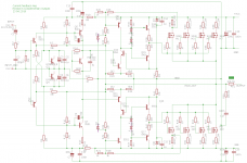
My preferred driver is much stronger, but in keeping with the minimalist design of the current feedback topology, I did not use it here. I post an example of a better driver below. [Caution, this is a paper design, exploring topology but not deep analysis of parts values, so this would need a once over before committing to building. I go fast when I am playing with a concept, and there may be errors I missed too.] I post this to show the better driver. There are many other differences from the topic of this thread. You will note that this has VI limiting. Also, the output stage has gain in order to allow rail to rail output. With complex loads, output stages with gain have problems. The infamous Tiger amps from the 70s used output stages with gain and suffered random failures, but I don't know the causes. You would want to overkill on the Zobel network to isolate reactive loads from this amp, and that concerns me. So, again, this is a paper design for discussion only.
Attachments
Last edited:
Could I take the functional aspects of the protection circuit here up to the clamp JFET and connect that to the gate of my CM?
Maybe. I did a quick runup of a design. However, I made it a switch only, no multiplier nor regulator. Why?
I feel the amp should be able to reject power supply hum and noise and regulated power is unnecessary. We make it so, by using effective circuit features in the amp, like RC filters on front end stages, differential inputs, current sources for differential pairs, and the like. A good regulated supply adds 30% to cost and wastes 30% of your power as heat, while reducing reliability. I don't feel that cost is justified if it is not necessary because the amp is already noise resistant. Your mileage may vary.
Once you have a MOSFET switch like this, you could easily make a regulator. Again, I chose not to do that.
Disclaimer: The circuit below is a paper design, unverified by an actual build. No simulation done. I present it as a concept vehicle only. It probably has holes. It's food for thought.
Attachments
The amplifier Output Zobel provides a load at high frequency so that an amplifier who's gain increase when presented with a near ininite HF load does not burst into oscillation.............You would want to overkill on the Zobel network to isolate reactive loads from this amp, and that concerns me. ................
The output inductor has the job of isolating the Load from the output stage and particularly from RF injected back into the NFB to -IN from the speaker and it's cabling.
Thank you slowhand. I might go ahead and make the detection and drive portion on veroboard and connect with flying leads to my Current Multiplier MOSFET (n-ch on positive rail, so will be connected to lower driver, and vice versa). So if I understand this, the opto-couplers serve to pull-up the gate during operation and gate is pushed-down with rail voltage (+ve to P-channel turns it off, -ve to N-channel turns it off). Switching should be very fast I gather.
Thank you slowhand. I might go ahead and make the detection and drive portion on veroboard and connect with flying leads to my Current Multiplier MOSFET (n-ch on positive rail, so will be connected to lower driver, and vice versa). So if I understand this, the opto-couplers serve to pull-up the gate during operation and gate is pushed-down with rail voltage (+ve to P-channel turns it off, -ve to N-channel turns it off). Switching should be very fast I gather.
No, the opto couplers connect gate to source, to shut off current. Normally the MOSFET gates are pulled up by the 1k resistor to turn on the pass elements, but if the thyristor fires the gates are clamped to ~1v and the MOSFETs turn off. I already found one bug in the connection of the optocouplers, and the current limit on the optocouplers needs some tweaks. See the fixed version below. Still I say beware, paper design, untested, concept only.
Attachments
X, thanks for the note on shipping the CHF9 GB boards. I will let you know if and when I receive the boards in Mexico. Since you shipped US priority mail, they may show up sooner than I think. The interesting part when they arrive will be trying to populate with products made from an electronics company here by the name of Steren Electronics. Fingers crossed.
Myles
Myles
X, thanks for the note on shipping the CHF9 GB boards. I will let you know if and when I receive the boards in Mexico. Since you shipped US priority mail, they may show up sooner than I think. The interesting part when they arrive will be trying to populate with products made from an electronics company here by the name of Steren Electronics. Fingers crossed.
Myles
This is for all GB folks. Please let me know when you receive the boards.
Hi X,
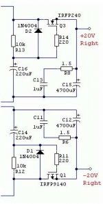
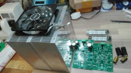
I recieve my boards today...thanks for all. I am going to populate them...and have a question : could you look under simulator the minimum Voltage rating of the two 2200uf capacitors in parallele with 10uf polyester one. I have 2200uf 6v3 nichicon FG in stock.
Marc
I recieve my boards today...thanks for all. I am going to populate them...and have a question : could you look under simulator the minimum Voltage rating of the two 2200uf capacitors in parallele with 10uf polyester one. I have 2200uf 6v3 nichicon FG in stock.
Marc
You can use 6.3v caps there even. I see maybe 1.5v max (2x factor of safety applied already)
Good to hear the boards arrived safely.
Good to hear the boards arrived safely.
I begin to collect parts from my stock......I don't think i will need the an : each heatsink mesure 200x165x80mm. I have matched IRFP pairs, and hfe matched BC556/546 as KSA1381 KSC3503.
Attachments
Last edited:
- Home
- Amplifiers
- Solid State
- CFH7 Amp