abetir, why not change R23 from 680 to 330 ohm?
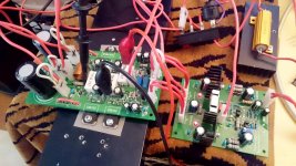
im testing attached where im using 330 ohm and both BDs run without heatsink.
(im testing with mains series bulb)(dont know if this is because of this).
Multisim tells me 700mW power dissip (they are 1.25W without heatsink).
Im very satisfied with the sound 😛
but im feeling that i need to remove the bulb in the mains and try without it 😀
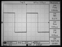
i am seeing unfocused sine when i attach the scope to its output. (think its from the bulb in the mains 😀 )
sound is crystal clear and brilliant, im wondering why its unfocused 😀
vzaichenko, do you know is this calculator correct ?
Guitar Pedals: R-C Filter Calculator
i know the formula but im too lazy and busy to calculate and compare.
1.25W is a maximum dissipation without a heatsink at 25 degrees ambient temperature, before it breaks, so better don't get too close to this limit. Even at 700mW, it will get considerably warm, increasing the ambient temperature - the output transistors will add to this at high power. You also don't take in account the rails voltage difference (35V vs 42V), so where you have 700mW, Albert will have 900mW. At this level of dissipation TO-126 device will be rather hot. Also, the heatsinks are recommended for the drivers as they ensure more stable bias for the output transistors in the end.
And finally - the purpose. Almost 12mA and and the low output impedance of the emitter follower is enough for driving 1 pair of HexFETs. Even good for 2 pairs.
Some 5 pairs - yes, you need the higher current, but then it would be better using at least TO-220 drivers to stay within the SOA at all times.
Unfocused curve on the scope most likely means some local oscillation.
And the last question about the RC calculator - you are too busy to compare, so do you assume I'm not busy enough to do it for you? 😕
This is ok now, maybe it was from the bulb in the mains it dropped the voltage to 30V.Unfocused curve on the scope most likely means some local oscillation.
And the last question about the RC calculator - you are too busy to compare, so do you assume I'm not busy enough to do it for you? 😕
I thinked you knew this calculator 😀
Dont even think about comparing for me.
abetir, im not having a vhex build, im having smth like it.
Last edited:

My boards arrived. I'm going to try this as a two output pair 100W amp in a compact chassis.
Cool! 😎🙂
VLatFET+
Albert and all,
I have just tested the similar front-end configuration together with Renesas lateral MOSFETs at the output, directly driven from the VAS stage (its quiescent current is increased up to 7mA for that purpose).
One or two pairs may be used (I have tested with 2 pairs and +/-52V DC rails).
Runs very smoothly, nicely sounding, thermally stable, no issues identified.
The whole thing is pretty fast, despite its overall simplicity 😉
Optimal quiescent current for the outputs is 100-110mA per pair (lowest distortion).
PCB may become even smaller now 🙂
Cheers,
Valery
Attachments
-
 DSC_0362.JPG469.5 KB · Views: 320
 -
 DSC_0361.jpg486.5 KB · Views: 158
 -
 DSC_0360.jpg740.5 KB · Views: 163
 -
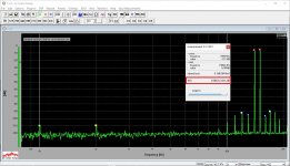 03-IMD-14-15KHz.JPG275.2 KB · Views: 183
 -
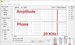
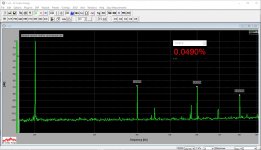 02-THD-20KHz.JPG174 KB · Views: 731
 -
 02-THD-01KHz.JPG181.8 KB · Views: 759
 -
 01 Bode 10Hz-100KHz.jpg105.2 KB · Views: 848
 -
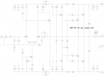 00-VLatFET-Sch-01.jpg291 KB · Views: 914
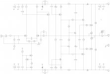
Is R15 (150r) intended to be different from R26 (75r)?
There is no capacitance after R20 & 21. Intended?
There is no capacitance after R20 & 21. Intended?
Is R15 (150r) intended to be different from R26 (75r)?
There is no capacitance after R20 & 21. Intended?
Yes, this is correct - Q5 and Q10 are the current sources, pulling the same current, but half of the current through R26 is taken by the collector of Q9, so R26 has to be half of R15 in order to keep the thing balanced.
Capacitance - yes, actually a couple of electrolytics can be added. Or C14-C17 can be moved after R20 & R21. In fact, this circuit has got rather high PSRR by design, so... I ran it the way it is - no ripple issues observed. Also - it's dead quiet, same as VHex one.
My boards arrived. I'm going to try this as a two output pair 100W amp in a compact chassis.
😎
 You won't be disappointed.
 A very good characteristic of VHex amp is that, even using local parts it still sounded very good and is dead silent.

Albert and all,
I have just tested the similar front-end configuration together with Renesas lateral MOSFETs at the output, directly driven from the VAS stage (its quiescent current is increased up to 7mA for that purpose).
One or two pairs may be used (I have tested with 2 pairs and +/-52V DC rails).
Runs very smoothly, nicely sounding, thermally stable, no issues identified.
The whole thing is pretty fast, despite its overall simplicity 😉
Optimal quiescent current for the outputs is 100-110mA per pair (lowest distortion).
PCB may become even smaller now 🙂
Cheers,
Valery


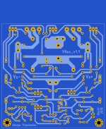
My take on VHex v1.1 (originally designed by Valery) I am only retaining the bigger horizontal mounted wirewound about the length of a Dale black wirewound resistor, so that both can be utilized.
I just thought it needs a rework 😉
Cheers!
Albert
I just thought it needs a rework 😉
Cheers!
Albert
Attachments
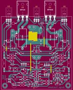
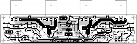
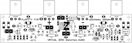
VLatFET+ (1 or 2 pairs of output devices) 7" x 1.5" inch layout
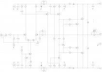
Here is a conpact SMD layout for the LetFET option - good for thin compartments or multi-channel builds.
Both VHex+ and VLatFET+ boards are available.
P.S. Rails decoupling is improved, AndrewT - thank you for raising this point earlier in the thread.
Here is a conpact SMD layout for the LetFET option - good for thin compartments or multi-channel builds.
Both VHex+ and VLatFET+ boards are available.
P.S. Rails decoupling is improved, AndrewT - thank you for raising this point earlier in the thread.
Attachments
I think, you mean single FET gate-to-source voltage - it can be around 3.7v for P-channel.
The question vas gate-to-gate. It's normally around 8V (4.2V for N-channel and 3.8V for P-channel).
thanks, this is all i wanted to know....
I have two V-Hex channels ready for testing, but I want to anodize the heat sinks before I crap them up with thermal compound.
Wow! Nice kit 😉
I have two V-Hex channels ready for testing, but I want to anodize the heat sinks before I crap them up with thermal compound.
wow, nicely done. can you tell me the part no. of i/p connector and its corresponding male part?
reg
Prasi
wow, nicely done. can you tell me the part no. of i/p connector and its corresponding male part?
reg
Prasi
That's the one:
Molex Connector Part Number - 39-28-1023
Part Number: 39-28-1023
Mini-Fit® Jr. Vertical Header, 4.20mm Pitch, Dual Row, 2 Circuits, without Snap-in Plastic Peg PCB Lock, Tin, Natural
Don't pay attention to the picture on that page - it's just a series picture of a 4-circuits connector. The one you need is 2-circuits.
There is also a link to the corresponding part on that page.
Cheers,
Valery
Thanks a lot for the link. Looks like an interesting thread, I will over the entire thread.
To JWilhelm,
A quick question, where is the sch located of the amp you posted a pic of?
reg
Prasi
Thanks a lot for the link. Looks like an interesting thread, I will over the entire thread.
To JWilhelm,
A quick question, where is the sch located of the amp you posted a pic of?
reg
Prasi
The exact schematic is not published here, although it's very similar to this one - >VHex with 1 pair of output devices< - but having 2 pairs of HexFETs at the output.
If you need the PCBs - we've got some available.
Thanks a lot for the link. Looks like an interesting thread, I will over the entire thread.
To JWilhelm,
A quick question, where is the sch located of the amp you posted a pic of?
reg
Prasi
Hi Prasi
Vzachenko did this layout. I don't think he ever posted the schematic, but it's the same as this with an extra set of output devices and associated parts.
http://www.diyaudio.com/forums/soli...-amplifier-simulated-tina-17.html#post4665097
- Home
- Amplifiers
- Solid State
- IRFP240/9240 Amplifier (simulated on TINA)