^not by actual hardware measurement, but in simulation, Valery can confirm that. Positive curent source trannie should be set ideally at 3.5ma and that gives 8ma at negative current source VAS trannie.
What does your sim say about the current across the two LEDs? I only ask because my two LEDs shine the same,
OK, I may have to simulate my actual components used in the circuit. I am using the larger 5mm types, I assume that current dissipation of CS trannie influences both LEDs. I have actually replaced it with a newer one, result is same brightness as the first one and zeners are of equal voltages. I do think it is a current issue.
Last edited:
@Valery,
Could this also be possbly an issue of the transistors being used?, which point to measure to best determine what influences the LED brightness? Bases of the trannies?
Sorry I had to ask as a newbie here.
Could this also be possbly an issue of the transistors being used?, which point to measure to best determine what influences the LED brightness? Bases of the trannies?
Sorry I had to ask as a newbie here.
Last edited:
@Valery,
Could this also be possbly an issue of the transistors being used?, which point to measure to best determine what influences the LED brightness? Bases of the trannies?
Sorry I had to ask as a newbie here.
Hi Albert,
Your current setup actually looks good, properly biased, no problem.
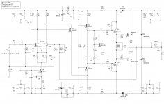
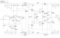
With regards to the LEDs. See how it works (schematic from post #93).
The current through both LEDs is set by R24 (base currents of Q4, Q5 are negligible - less than 30uA - they can be ignored). So, current through the LEDs is the same by design. The fact one of them shines brighter - I think, some LEDs just shine brighter than the others. Nothing to worry about.
VAS current is the same for both shoulders - positive and negative.
You can measure the voltage over R8 and R17. The voltage will be roughly the same (1.1-1.3V), but the value of R8 is twice as high, comparing to the value of R17 - that's because half of the current through R17 is consumed by Q3 - that's how the current drive actually works.
Cheers,
Valery
Thanks guys,
I am in the process of populating the other channel and I just had the 3mm LEDs. Once completed I will let you know.
Cheers!
Albert
I am in the process of populating the other channel and I just had the 3mm LEDs. Once completed I will let you know.
Cheers!
Albert
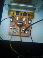
Here is my 2nd channel, all LEDs brightly shines. 🙂
I used 2sd669/b649 for Q3,4 & 5. It worked fine but I thought the superfast CRT vertical deflection transistor sounds much better here. VAS sink is DIY made , I just hammered the thing into shape just to have it made quickly.😀
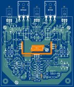
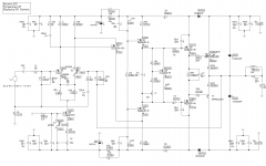
I am reposting here my PCB lay-out , now with the corrected traces and parts orientation and an option to install a single 1watter 1.8k for the input supply. My parts implementation is a combination of both the first VHex schematic (post #93) and the later VHex v1.1 (post #164)
Cheers!
Albert
I used 2sd669/b649 for Q3,4 & 5. It worked fine but I thought the superfast CRT vertical deflection transistor sounds much better here. VAS sink is DIY made , I just hammered the thing into shape just to have it made quickly.😀
I am reposting here my PCB lay-out , now with the corrected traces and parts orientation and an option to install a single 1watter 1.8k for the input supply. My parts implementation is a combination of both the first VHex schematic (post #93) and the later VHex v1.1 (post #164)
Cheers!
Albert
Attachments
Last edited:
And your hand made sink for the three transistors looks very effective for the dual duty of cooling and maintaining a near equal environment temperature.

Thank you guys!
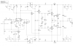
This all BDs TO-126 simulation is an answer to Peter Basel's query on post # 158 and Terry's query on my LED currents at post # 202 (excepting Q3 which is ideally 2SC1381).
I just thought it is worth noticing as a reference as BD devices is one of the more popular parts used by DIYers in the forum. Schematic follows the latest v1.1 at post # 164 Simulation is 1v amplitude at 1KHz freq. You may notice DC offset is negative as it displays more closer equal current dissipation of the input pair and the output ballast resistors than on having a positive dc offset. IRFP240 is a generic model this explains why it shows a different symbol than the IR 9240 model.
Cheers!
Albert
Attachments
abetir, why not change R23 from 680 to 330 ohm?
im testing attached where im using 330 ohm and both BDs run without heatsink.
(im testing with mains series bulb)(dont know if this is because of this).
Multisim tells me 700mW power dissip (they are 1.25W without heatsink).
Im very satisfied with the sound 😛
but im feeling that i need to remove the bulb in the mains and try without it 😀
i am seeing unfocused sine when i attach the scope to its output. (think its from the bulb in the mains 😀 )
sound is crystal clear and brilliant, im wondering why its unfocused 😀
vzaichenko, do you know is this calculator correct ?
Guitar Pedals: R-C Filter Calculator
i know the formula but im too lazy and busy to calculate and compare.
Attachments
Last edited:
thanks, data sheet says 2 to 4 volt gate thresholds so that 5 volts fall within the 4 to 8 volts possible spread, wonder if any other build gets it at lower than 4 volts...
abetir, add an OLED display oscilloscope to this project 😀
https://www.youtube.com/watch?v=XHDNXXhg3Hg
Ive ordered one and now im waiting 1 month. (4$ from aliexpress)
You can monitor rails or output realtime 😛
https://www.youtube.com/watch?v=XHDNXXhg3Hg
Ive ordered one and now im waiting 1 month. (4$ from aliexpress)
You can monitor rails or output realtime 😛
Last edited:

guys, can you post the actual gate to gate bias voltage in your working amps?
My build had 3.7v on both channels. 🙂
@mosfet54,
Post the images of your VHex build, so that others may see it too. 😉
...and I suggest we stick with the VHex amp discussion.
Thank You!
My build had 3.7v on both channels. 🙂
@mosfet54,
Post the images of your VHex build, so that others may see it too. 😉
...and I suggest we stick with the VHex amp discussion.
Thank You!
I think, you mean single FET gate-to-source voltage - it can be around 3.7v for P-channel.
The question vas gate-to-gate. It's normally around 8V (4.2V for N-channel and 3.8V for P-channel).
- Home
- Amplifiers
- Solid State
- IRFP240/9240 Amplifier (simulated on TINA)