Interesting
A friend and I have been considering something like this, but with mirrored sides for the phases. The shift registers could be installed upside down.
A friend and I have been considering something like this, but with mirrored sides for the phases. The shift registers could be installed upside down.
Perhaps I'm being too compulsive, but I've re-layout the board so that the BCLK has a constant path length to the shift register chips:
View attachment 514826
In this case the clock and DSD signals come in via U.FL. This board is for each channel.
Perhaps I'm being too compulsive, but I've re-layout the board so that the BCLK has a constant path length to the shift register chips:
Hi ... I can't speak for your being compulsive ( ;-) ) but I did the same with the DSD DAC I've made. If my calculations are not erroneous even a difference of a millimeter means picoseconds difference between the time the clock arrives at two different chips. And although this time difference is not random (like jitter could be) I considered it worthwhile to eliminate. So IMHO it makes sense to me ...
Cheers,
Jesper
A friend and I have been considering something like this, but with mirrored sides for the phases. The shift registers could be installed upside down.
Nice idea! That reduce the BCLK path length on the board.
That, and it helps with common mode rejection on the balanced signals. I would love to see this as a simple board with no I/V after the networks for going into a very high quality balanced transformer. I'd go in on it with someone who also wants something like this to split the board costs.Nice idea! That reduce the BCLK path length on the board.
Last edited:
JLSounds
Does anyone have the JLSounds I2SoverUSB working on DSD256 using OSX or Windows? I just received one, and cannot get it to do native (non DoP) DSD which limits me to DSD128. Miska states that the DSC1 is optimized for DSD256+. So far, the JLSounds sounds A LOT better than my Amanero. Full disclosure: I have never cared for the signature of the Amanero, and for all I know, mine has a bad clock or something. It does however, work as described! LOL
Does anyone have the JLSounds I2SoverUSB working on DSD256 using OSX or Windows? I just received one, and cannot get it to do native (non DoP) DSD which limits me to DSD128. Miska states that the DSC1 is optimized for DSD256+. So far, the JLSounds sounds A LOT better than my Amanero. Full disclosure: I have never cared for the signature of the Amanero, and for all I know, mine has a bad clock or something. It does however, work as described! LOL
Last edited:
That, and it helps with common mode rejection on the balanced signals. I would love to see this as a simple board with no I/V after the networks for going into a very high quality balanced transformer. I'd go in on it with someone who also wants something like this to split the board costs.
Well theoretically yes but there are additional digital realities that make this a choice with several tradeoffs (perhaps these issues can be resolved?):
How to get the clock to the backside of the board without vias? vias are contraindicated for clocks, no? Also you'd almost need a 6 layer board because you can't easily route the signals without using two layers, currently I have:
top (layer 1): signal: chips and clock
GND
layer 3: signal
bottom: VCC
and if we start routing signals in the ground plane, thats not ideal.
you'd be best off with:
top: chips and signal
GND1
signal 2
VCC
signal 3
GND2
bottom: chips and signal
and you still need vias for clock so, worth it?
Alternatively could build 2 4 layer boards and stick them together back to back -- maybe pin that runs through all 4 boards to distribute clock rather than U.FL connection?
The issue regarding common mode rejection is that the chips, and hence traces, are not directly mirrored so does that still help?
How about the network and 595s on one daughter board


Yes, that is the idea. That way we can use different I-V and filter sections. For the balanced version I'm putting a D flip flop on board.
Question is: best way to get high quality clock to board? U.Fl splitter could distribute two micro cables to right and left sides, or stack boards and run a pin down the middle?
Sent from my iPhone using Tapatalk
Question is: best way to get high quality clock to board? U.Fl splitter could distribute two micro cables to right and left sides, or stack boards and run a pin down the middle?
Sent from my iPhone using Tapatalk
Very...
Interested in this approach for a balanced DAC. I suspect that it will be best to wait until a clock distribution/digital specialist can be consulted on how to best distribute the clock signal. Too bad Pat is banned from here, I bet Demian Martin would know how best to approach this.
Yes, that is the idea. That way we can use different I-V and filter sections. For the balanced version I'm putting a D flip flop on board.
Question is: best way to get high quality clock to board? U.Fl splitter could distribute two micro cables to right and left sides, or stack boards and run a pin down the middle?
Sent from my iPhone using Tapatalk
Interested in this approach for a balanced DAC. I suspect that it will be best to wait until a clock distribution/digital specialist can be consulted on how to best distribute the clock signal. Too bad Pat is banned from here, I bet Demian Martin would know how best to approach this.
Interested in this approach for a balanced DAC. I suspect that it will be best to wait until a clock distribution/digital specialist can be consulted on how to best distribute the clock signal. Too bad Pat is banned from here, I bet Demian Martin would know how best to approach this.
I'm interested in getting expert advice.
Here is my latest version:
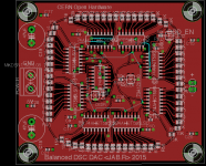
The BLCK enters the center by u.fl, terminated by 50 ohm and the the traces fan out in a curved fashion. The upper 4 595s are the (+) side and the bottom (-), the D-flip flop is to the immediate left of the BLCK center.
The board is 2.8x2.44 inches in dimension.
Do we handle GHz?
4 layers: signal - power - power - signal.
595 as mezzanine to reduce overall length (using Z for placing).
You can use clock distribution IC as done in PC for PCIe...
And yes, best would be a good transformer instead OPAMP I/V.
Jean-Paul
4 layers: signal - power - power - signal.
595 as mezzanine to reduce overall length (using Z for placing).
You can use clock distribution IC as done in PC for PCIe...
And yes, best would be a good transformer instead OPAMP I/V.
Jean-Paul
Do we handle GHz?
4 layers: signal - power - power - signal.
595 as mezzanine to reduce overall length (using Z for placing).
You can use clock distribution IC as done in PC for PCIe...
And yes, best would be a good transformer instead OPAMP I/V.
Jean-Paul
No GHz but with DACs there is a desire to have a low jitter clock, and so it is generally considered good to optimize this circuit. iancanada's Dual XO clock board does, I believe, use a distribution IC but unclear how many outputs it has (u.fl connections), that is for this circuit would need connection to both R and L boards. I'm also building R2R DAC for PCM signals and so would need R and L also.
Would you propose one distribution IC to go between the reclock module and the DAC boards and then a second IC on each board to distribute to the individual chips?
Would mezzanine reduce overall length? What distance do you have it down to? Tradeoff between that and right angle connectors?
I have a FirstWatt M2 and yes it will be interesting to see how that works directly following DAC. Also have a bunch of Edcor xformers on way🙂 It would be nice to plug in different I-V and filter modules to see what sounds best.
Last edited:
potato clock distribution
I added the potatosemi 1:10 clock buffer IC
iancanada's Dual XO II uses a dual potato semi flip flop as the output buffer. The 1:10 chip has reasonable specs including <100 ps part to part skew. 9 lines are needed, 1 for the d-flip-flop and 8 for each of the shift register chips.
The clock distribution path lengths are 17.2 +/- 0.2mm (just in case you want to run a 17ghz clock 🙂
This version uses VCC=3.3V
layers: signal, GND, VCC, signal
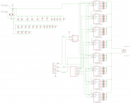
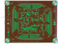
Comments?
I added the potatosemi 1:10 clock buffer IC
iancanada's Dual XO II uses a dual potato semi flip flop as the output buffer. The 1:10 chip has reasonable specs including <100 ps part to part skew. 9 lines are needed, 1 for the d-flip-flop and 8 for each of the shift register chips.
The clock distribution path lengths are 17.2 +/- 0.2mm (just in case you want to run a 17ghz clock 🙂
This version uses VCC=3.3V
layers: signal, GND, VCC, signal


Comments?
0603 resistor?
What Eagle Version used?
Jean-Paul
only 0603 for termination, the resistor ladder are 0805s.
Eagle 7.5.0.
I would use 0603 for ladder (better 595 fan-out --> better routing)?!
What is your Z0 value?
Jean-Paul
What is your Z0 value?
Jean-Paul
I would use 0603 for ladder (better 595 fan-out --> better routing)?!
What is your Z0 value?
Yes, more work for our sore eyes but thats why we have microscopes and placement with tweezers is good therapy 🙂
The Susumo RG comes in both: RG1608N-153-W-T1
Unsure the Z0 as its not on the datasheet.
mcxlun had good results with this part, and thats where I got started off with the 0805s -- those little network boards🙂
Last edited:
I mean the impedance Z0 of your differential pairs. The impedance also for the clock routing?
Jean-Paul
Jean-Paul
Use as much as possible vias for GND planes connecting, supposing coplanar routing.
Nice link:
Saturn PCB Design - PCB Via Current | PCB Trace Width | Differential Pair Calculator | PCB Impedance
Jean-Paul
Nice link:
Saturn PCB Design - PCB Via Current | PCB Trace Width | Differential Pair Calculator | PCB Impedance
Jean-Paul
I mean the impedance Z0 of your differential pairs. The impedance also for the clock routing?
There aren't any differential pairs. The input cables (u.fl) are 50ohm and the traces look like they are 65 ohm.
- Home
- Source & Line
- Digital Line Level
- Signalyst DSC1